The PCB outline, fitted with a 3D print
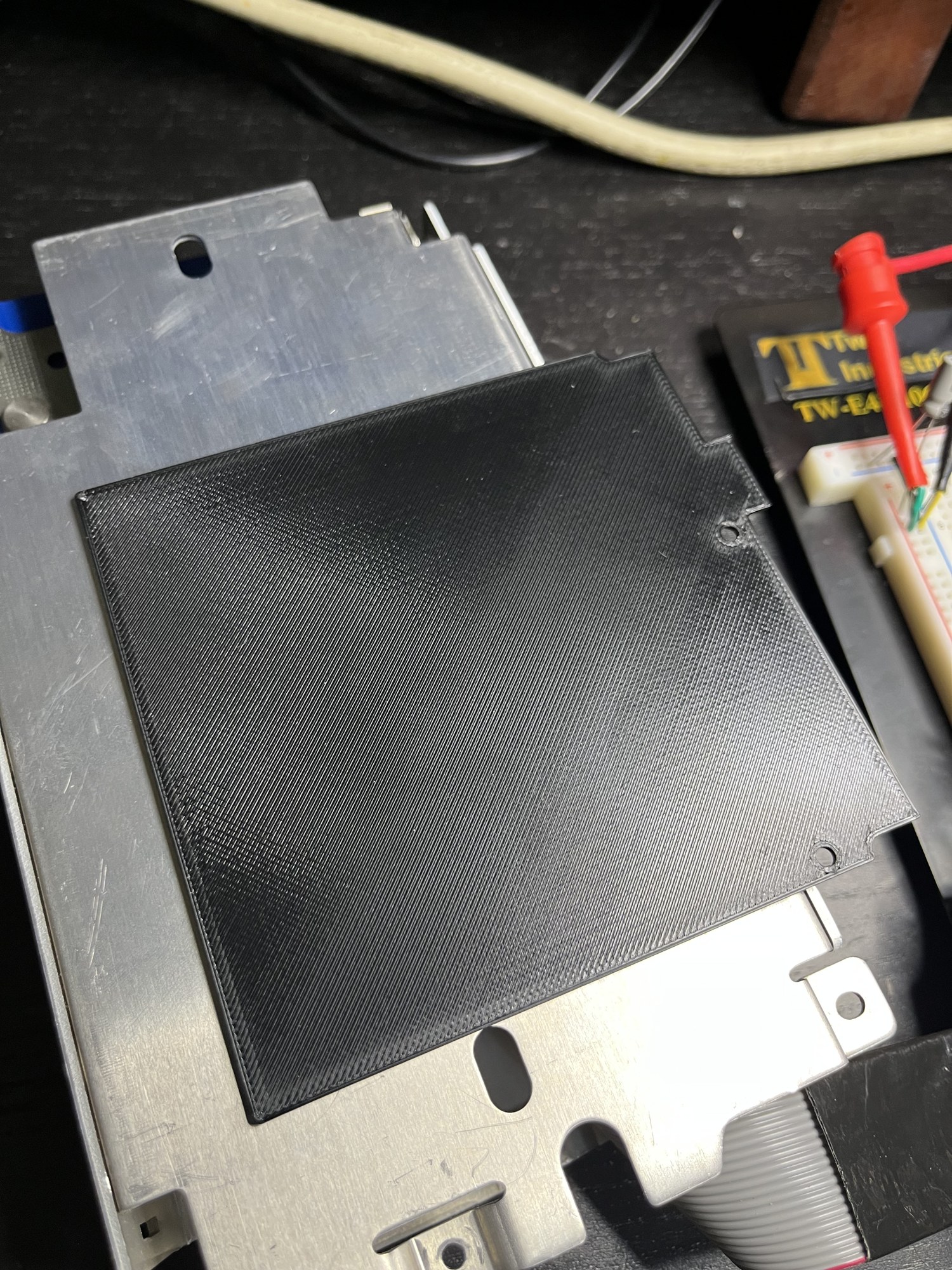
The replacement PCB has an outline now, and a 3D-printed copy of it lines up with both mounting holes on the original IF-83. Everything on the new board has to fit inside this shape.
Ruler numbers off a photo
I started with a photo of the IF-83’s solder side and a ruler. My first read was 100 mm wide, 105 mm tall, a 95 mm section across the top, and a 10 mm tab about 20 mm in from one side.
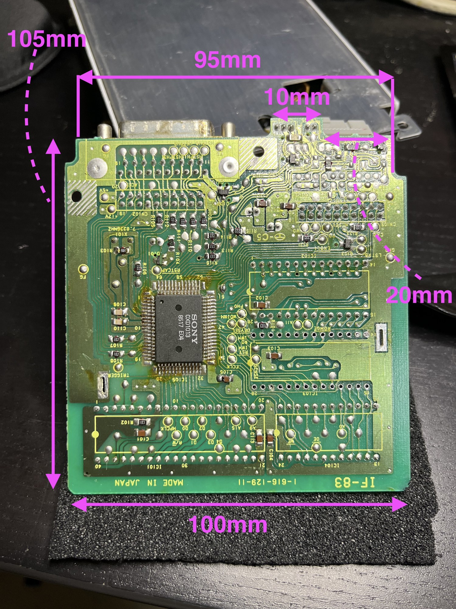
The photo shows the solder side, so the outline in KiCad is the mirror image of it. The tab that sits on the right in the photo is on the left when you look at the component side.
Use calipers to copy a board outline
The ruler got me close enough to draw something and far enough off to matter. When I went back over the board with calipers, most of the numbers moved.
| Feature | Ruler | Calipers or print |
|---|---|---|
| Top section width | 95 mm | 94 mm |
| Tab width | 10 mm | 15.5 mm |
| Tab position | about 20 mm in | 22 mm from the top section’s edge |
| Tab height | 5 mm | |
| Mounting hole | 4 mm | about 3.35 mm, so M3. Drawn at 3.2 mm. |
The tab was the biggest miss. The ruler said 10 mm and the calipers said 15.5 mm.
The steps aren’t level
The top section is narrower than the body and steps out to 100 mm on both sides with a shallow curve. I drew both steps at the same depth. Laid on the board, the left one needed to come up 2 mm and the right one to go down 3 mm, so they’re 8 mm and 13 mm below the top edge (component side). Nothing in the chassis sits there, so the steps are only about matching the original.
One hole was 3 mm low
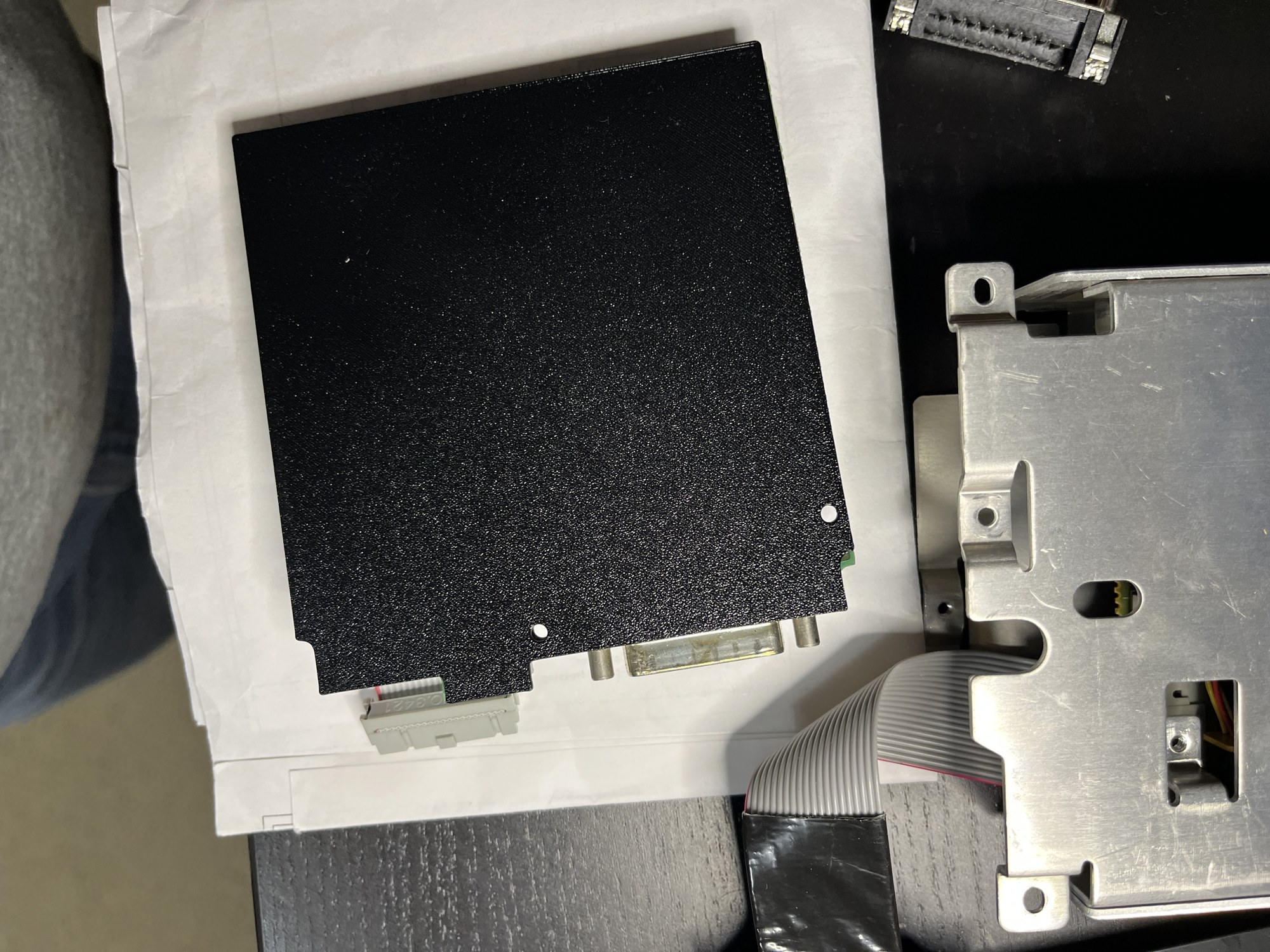
The hole next to the tab was right on the first print. The other one was 3 mm too low and 0.5 mm too far in from the board edge. After moving it, both holes line up with the IF-83. Stacked on the original board, the white paper under it shows through both holes.
| Hole | Position (component side) |
|---|---|
| Next to the tab | Center 40 mm from the top section’s left edge, hole edge 3 mm below the top edge |
| Side | Hole edge 1.5 mm from the board edge, center 17 mm below the top edge |
It has to be hand-solderable
I want to build this board with an iron. That rules out QFN, BGA and anything with a pad underneath, and sets 0.65 mm as the finest pitch, with 1.27 mm SOIC preferred. The level shifters will be SN74LVC8T245DWR, the wide SOIC-24 version of the part on my prototype boards. The bare RP2350A is a 0.4 mm QFN-60, so the board carries a Pico 2 soldered flat by its castellated edge pads, with no headers, to keep the board as flat as possible.
Still open
- The DB-19 screw holes and any other holes aren’t drawn yet.
- The step curves were copied by eye from the photo.
- Next is the schematic, then fitting the parts inside this outline. The Pico 2’s USB end needs to sit at a board edge, and its SWD pins need to stay reachable.