Going around the CXD1013
I have two UniDisk 3.5 drives (A2M2053) with dead controller boards and one that works. The mechanisms in the dead ones are fine. I ran both on the working board a few months ago, and one of them is refurbished and regreased. On an Apple IIe the UniDisk is the only way to get 3.5" disks, and the one spare controller board on eBay has been sitting at $150 for about seven months. So I’m building a replacement board.
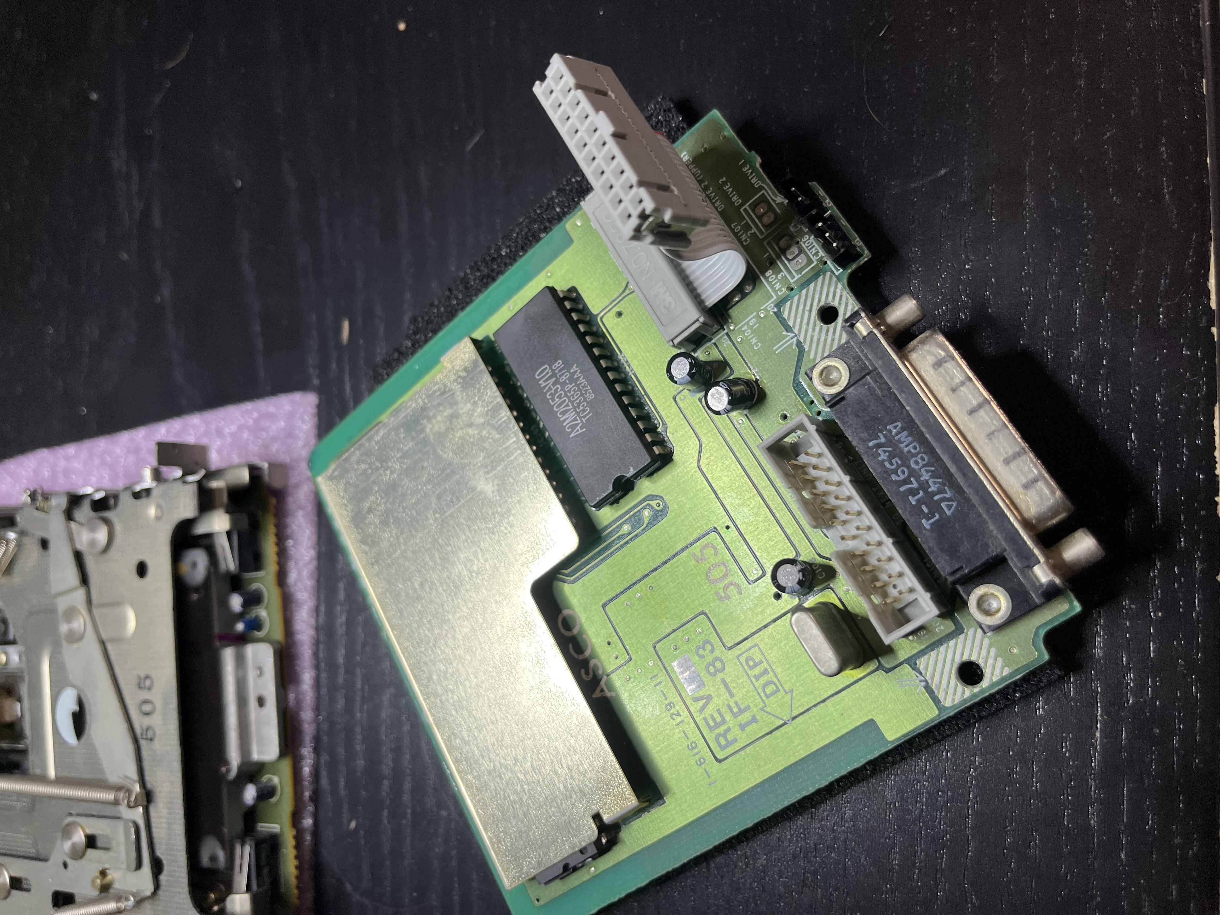
Nobody has anything on the Sony CXD1013
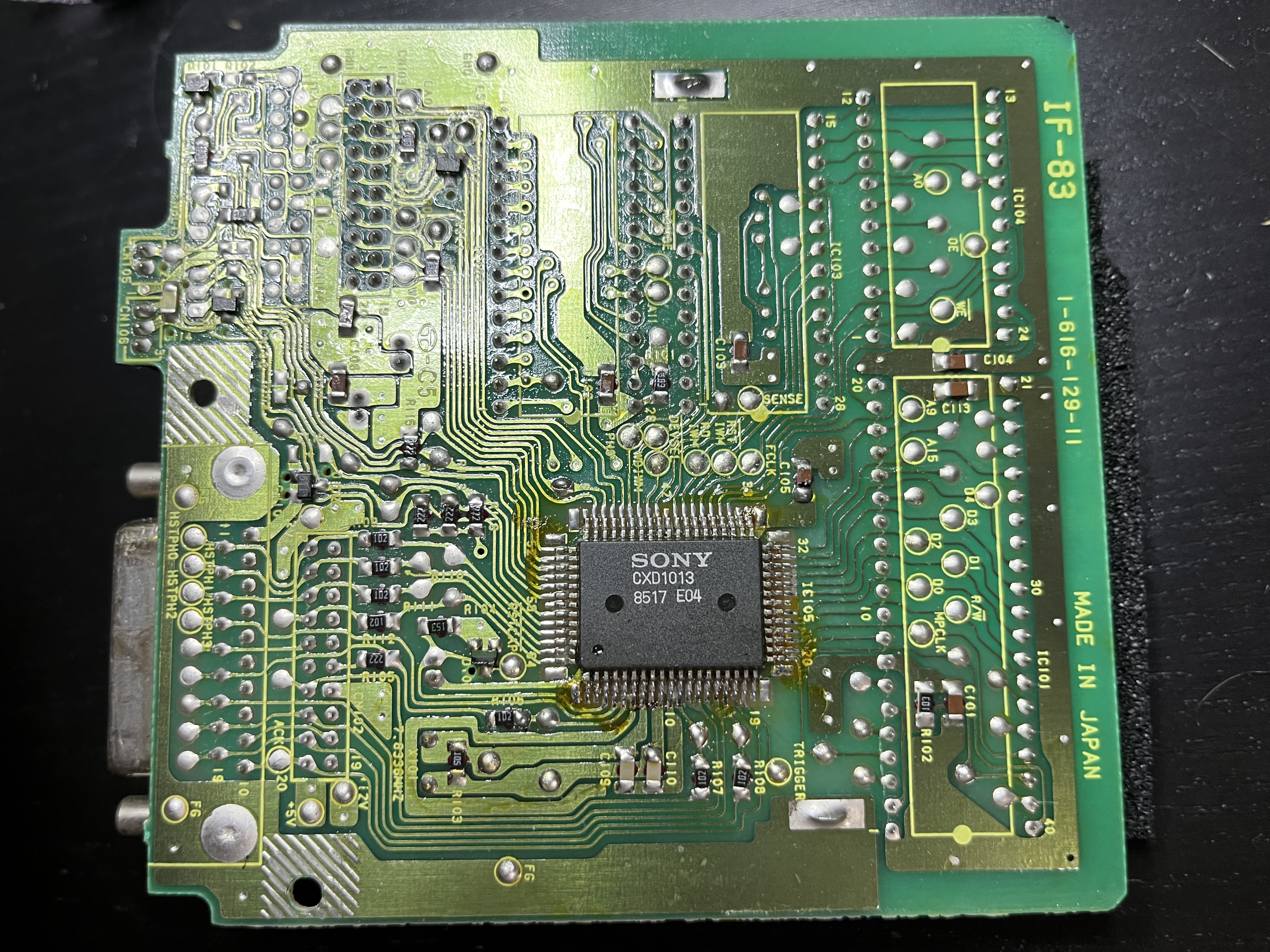
The controller board (IF-83, service part 661-0307) is a 65C02, a mask ROM, 2K of RAM, an IWM, and a Sony CXD1013 gate array on the bottom. The gate array is the problem. I emailed Sony and they said they have nothing on it. The Computer History Museum never answered. Without a known-good spare chip there’s nothing to reverse engineer against.
| Ref | Part | Job |
|---|---|---|
| IC101 | GTE G65SC02P-2 | CPU, 2 MHz |
| IC102 | Toshiba TC5365P, “A2M2053-V1.0” | 8K ROM at $E000 |
| IC103 | AMI 344-0041-B | IWM |
| IC104 | Sony CXK5816PN-12L | 2K SRAM at $0000 |
| bottom | Sony CXD1013 | gate array, no datasheet |
The drive ROM already explains the gate array
Byte Hamr’s repo has Eric Smith’s 2018 disassembly of the drive’s own 65C02 firmware (liron.asm, next to the Liron card ROM). It maps the gate array as two registers at $0800 and $0801, with bits named LASTONE, BUSEN, WRREQ, HDSEL, SENSE, BLATCH, IWMDIR, PH3EN, ENBUS and DRIVE1/2. One IWM gets switched between the SmartPort side and the mechanism by the IWMDIR bit. The ROM sets the IWM mode to $1F (fast, 2 us cells) for the mechanism and $17 for SmartPort.
That means I don’t need the CXD1013 at all. I need to drive the mechanism connector myself and use the ROM as an oracle for sequences and timing: seek, recal, eject retries, and the SmartPort command and status tables.
The mechanism is a Mac 800K drive on a 20-pin header
Bitsavers has Apple’s engineering spec for the 800K double-sided drive (699-0321, August 1985). It has the 20-pin connector pinout, and the silkscreen next to CN104 on the controller board matches it: CA0, CA1, CA2, LSTRB, SEL, /ENBL, RD, WR. The mechanism handles its own speed in five zones, so the controller never has to drive PWM.
If you’re trying to drive a UniDisk 3.5 mechanism without its controller: CN104 is the Mac 800K drive’s 20-pin interface, status comes back on RD selected by CA0-2 and SEL, and pin 20 (/PWM) is tied straight to +5V on the original board. I checked pin 20 with the meter.
| Tracks | RPM | Sectors per track |
|---|---|---|
| 0-15 | 394 | 12 |
| 16-31 | 429 | 11 |
| 32-47 | 472 | 10 |
| 48-63 | 525 | 9 |
| 64-79 | 590 | 8 |
Data rate is 489.6 kbit/s. The OCR’d spec is unreadable at the 472 RPM entry, so that one is the standard Mac 800K value. The mechanism board has its own Sony chips: a CX23077A dated 8515 and a CX20185, which is the read/write head amp. The power pins are +5 V and +12 V only, so the bench needs two rails.
Rear port continuity off a dead board
The daisy-chain port on the back mostly passes straight through to the host header CN102. Three pins go into the CXD1013 instead.
| Rear DB-19 | Goes to | What it is |
|---|---|---|
| 9 | CN102 pin 17 | HDSEL, pass-through |
| 10 | CN102 pin 20 | WRPROT/ACK, pass-through (pin 20, not 19) |
| 14 | CXD1013 pin 4 | PH3 to the next drive, gated |
| 16 | resistor to CXD1013 pin 5 | LASTONE sense |
| 17 | CXD1013 pins 12 and 13 | /ENBL to the next drive, gated |
The pin 16 trick is in an Apple handwritten pin table from 1985 that’s bundled with the Apple 3.5 Drive schematic on bitsavers: “GND on input port, +5V 2k on output port.” A drive plugged in behind you grounds it, so the drive knows whether it’s last in the chain.
The plan
An RP2350 on a Pico 2 does everything. One PIO block runs SmartPort, ported from the PicoPort code that already boots ProDOS on the Byte Hamr side. The other PIO block times flux on the mechanism’s RD line and writes GCR. Level shifting is five of my SN74LVC8T245 boards. Each one has a single DIR and /OE, so signals get grouped by direction and by when they need to be enabled. The pin count comes out at 25 of 26 GPIO with daisy chain included.
Scope is the Apple IIe and 800K ProDOS disks. The UniDisk docs talk about Mac disks and 400K, and the ROM still has single-sided format code, but the IIe never used either.
Firmware gets done one milestone at a time with a bench stop after each: M0 rig and boot safety, M1 status bits, M2 motor, seek and eject, M3 raw flux capture and a full disk read compared byte for byte against an image made on the working drive. Writing comes later at M5. The M0 scaffold firmware builds and its host tests pass. It sets every mechanism line to its idle level and holds the shifter’s /OE high before USB comes up. I also grabbed Raspberry Pi’s prebuilt OpenOCD, because the one I had only knew the RP2040.
Cable breakouts
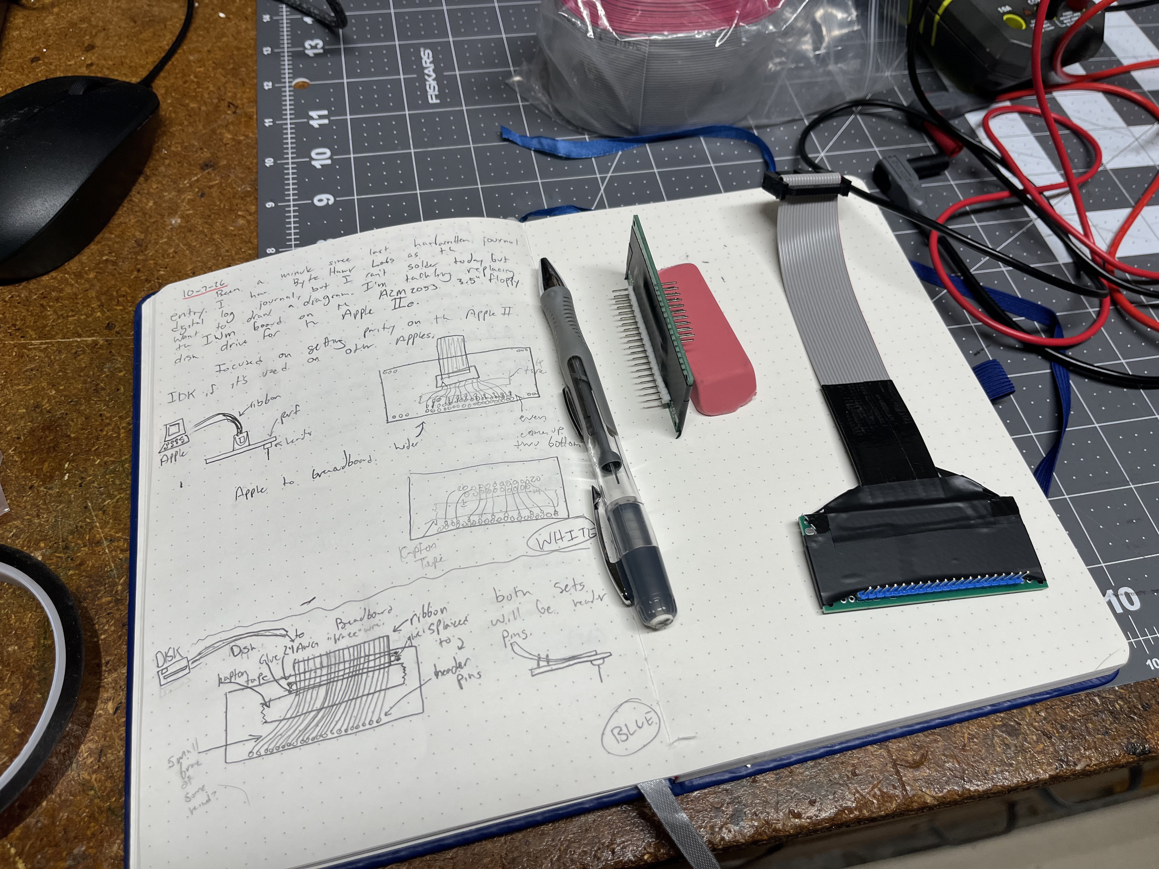
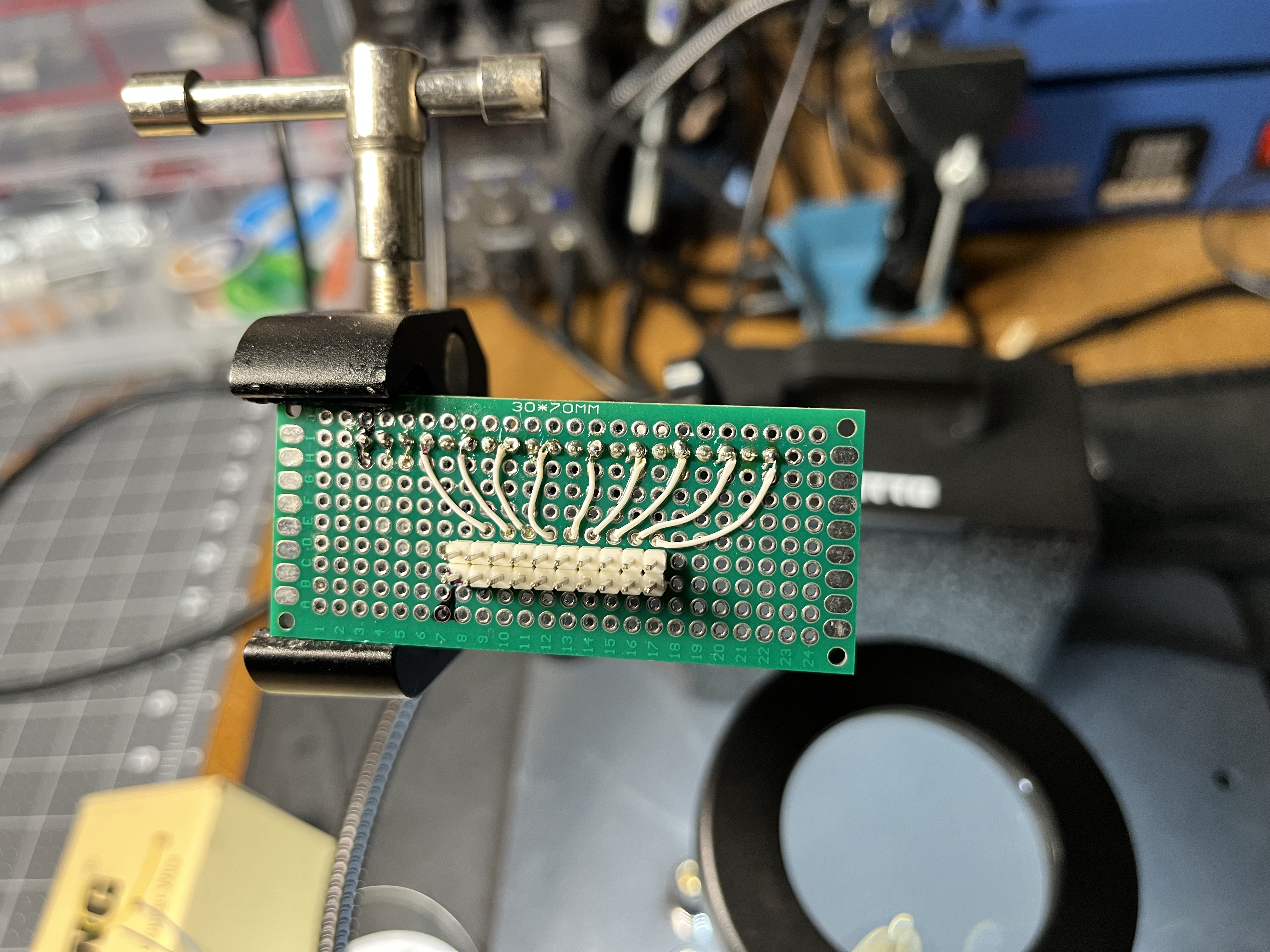
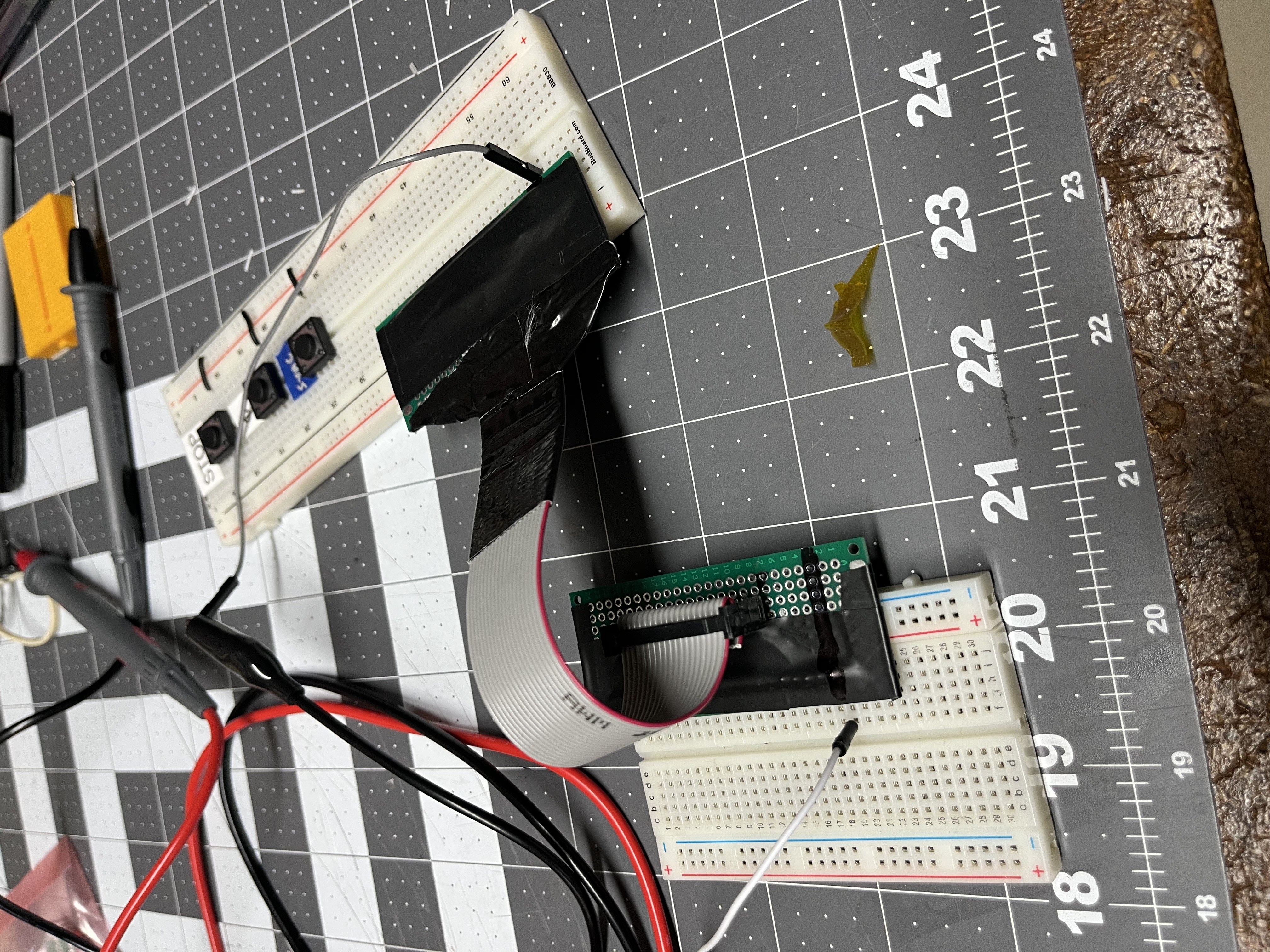
The first hardware is two adapters that take the 20-pin cables down to header pins for the breadboard, one for the disk cable and one for the Apple side. Both are 30x70 mm perfboard wired with 32AWG. Soldering 32AWG is tedious and this took a lot longer than I wanted. All the beep checks passed.
Open threads
- M0 still needs the Pico 2 and the first two shifter boards wired, a mechanism-only power test with the Pico unplugged, then a scope check that /OE and LSTRB stay put through a reset.
- My picoprobe may need newer debugprobe firmware to talk to the RP2350.
- I need a reference 800K disk made on the working UniDisk and imaged over ADTPro before M3.
- 3.5" GCR has no index pulse, so writes have to find the sector header on the fly and switch the write gate on inside the gap. Write precompensation isn’t in any doc I have.
- The rule for passing /ENBL down the daisy chain is my reading of the ROM. It gets checked with the working drive plugged in behind the new board.
Sources: bitsavers Sony/Apple drive docs, tashnotes for the GCR checksum and MCI tables, and Eric Smith’s disassembly in the project_byte_hamr repo.