Disk Hamr: the PCB is routed
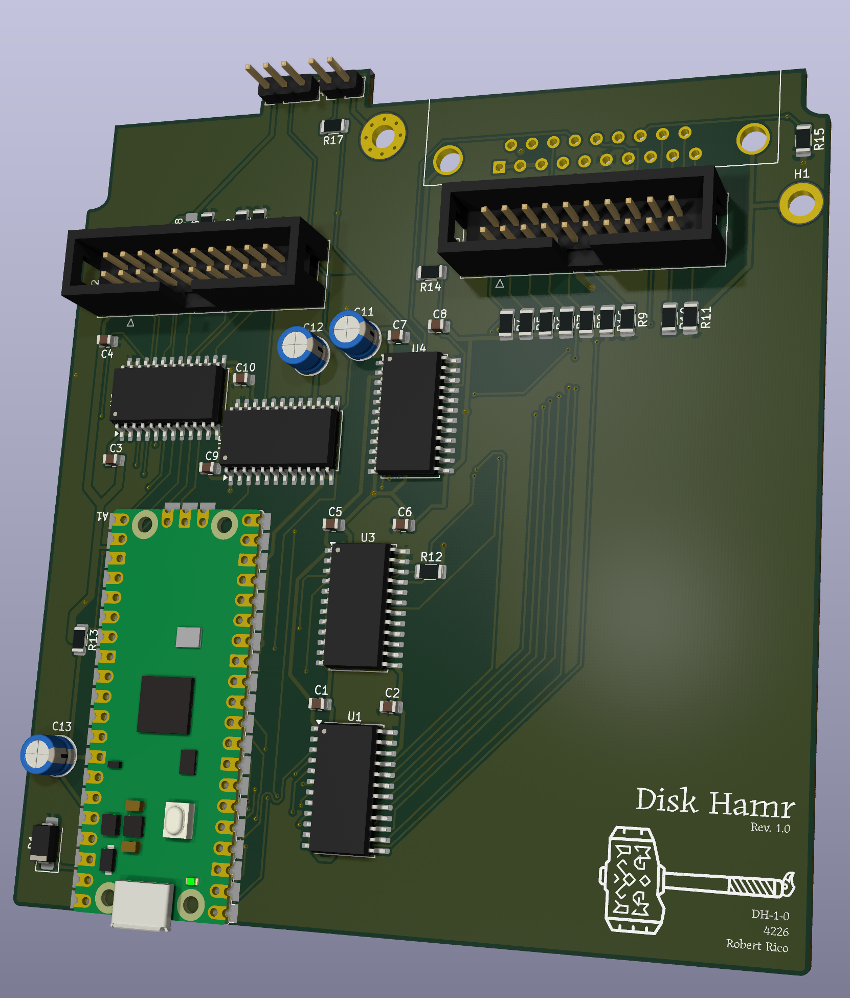
The board has a name now, Disk Hamr, and a finished layout. 100 x 110 mm, two layers, 46 parts, all on top. Same shape as the 3D-printed outline that fitted the IF-83’s mounting holes and the case opening in M7.
Schematic changes before layout
Three things moved in the schematic so the board could be routed sanely.
- R18, a 10k pull-down on LSTRB to ground. The breadboard had that resistor to +5 V by mistake, and it still worked, which says something about the CX23077A’s input. It’s to ground now, on the rig and on the board.
- Eight shifter channels re-ordered. The 8T245s don’t care which channel carries what, so I let the layout pick. LASTONE/, /HSTEN and WR moved on U1, mech RD on U5, and the four CA/LSTRB lines on U2 are reversed so the fan-out to the Pico doesn’t cross itself. The prototype gets rewired to match before I order boards.
- FG is gone. I’d made up a frame-ground net while fit-testing the DB-19 and the mounting holes. Frame ground is ground. The two M3 holes and the DB-19 shell are on GND, schematic and board.
Routed twice
Round one was Claude driving KiCad through Konnect, an MCP bridge to KiCad’s IPC API. It routes one straight segment per call, no push-and-shove, no 45 degrees, and no idea what copper is already under the cursor unless it asks. It got there: DRC clean, every net connected, the power laid out the way I wanted. It also left 112 vias, right angles everywhere, and a few runs that went straight through things it hadn’t looked at. Fine for a prototype, ugly to look at.
So I tried Freerouting 2.5 for comparison. The first attempts were bad for reasons that had nothing to do with the board. I’d locked the power routing and left the pours in, and Freerouting saw a pour on each layer, decided both were power planes, and routed around them. It quit in a few seconds with 49 connections open and 102 new vias. With the pours hidden from it but the locks still on, it counted every ground pin as unrouted and gave up faster.
Wiped clean, no tracks, no vias, no pours, every net to route, it finished everything in 12 seconds, zero violations, 73 vias. That one I imported.
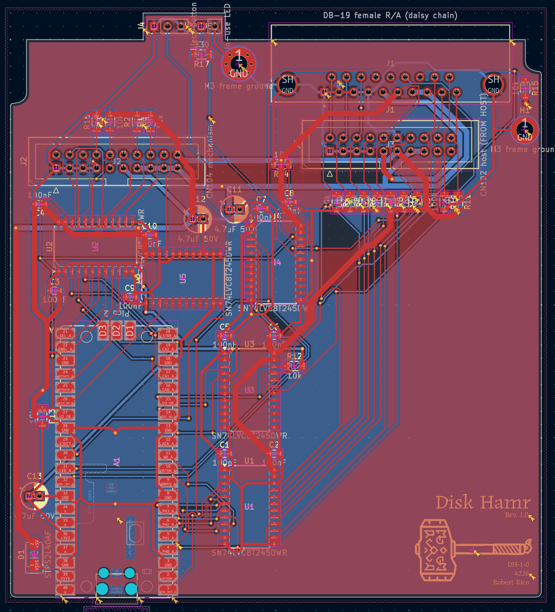
The import needed hand work. Freerouting necks traces down where they enter a pad narrower than the trace, and it wrote fifty 0.187 mm stubs that way, under KiCad’s 0.2 mm minimum. Two pieces of ENBL_OUT didn’t survive the round trip. Four ground traces ran inside the board-edge clearance. And with no plane to lean on it had drawn ground as 630 mm of traces, so I dragged vias in by hand to stitch the IC ground pins to the plane. One catch the pour refill found: the mechanism’s +5 group, J2 pins 11 and 20, its bulk cap and the U5 feed, was an island. The SEL, ENBL and WRTDATA drops walled it off on top and the +12 band sat above it. A 1.2 mm run on the bottom from that strap over to the host +5 feed closed it.
| Hand-routed | Freerouting, fixed by hand | |
|---|---|---|
| Segments | 415 | 870 |
| Vias | 112 (37 ground stitches) | 84 |
| Bottom-layer tracks cutting the ground plane | 899 mm | 1001 mm |
| Ground as traces | 133 mm | 630 mm |
| 45-degree segments | 42 | 365 |
| DRC | 0 errors, 0 unconnected | 0 errors, 0 unconnected |
A wash on vias and plane cuts, a clear win on looks and on time. The hand-routed board stays in the repo history.
Power
The +5 lesson from M8 is in copper now. +5 is a pour over the whole top layer; ground is a pour over the whole bottom. +12 gets its own band on the top layer where it crosses from the host header to the mechanism header, carved out of the +5 pour, with a 1 mm bottom-side jumper under the mechanism’s RD trace at the one place it couldn’t stay on top. The +5 and +12 runs between the two headers are 1 mm, the rails to the rear DB-19 the same. The host pull-ups sit in strips of the +5 pour walled in by the bus columns, so a bus on the bottom ties them in.
The one thing I’d still change: between the two headers the 1 mm +5 and +12 bottom-side runs sit side by side and cut a 30 x 4 mm slot out of the ground plane, right across the mechanism-to-host return. The plane is still one piece around it. Prototype.
Checks
| Check | Result |
|---|---|
| DRC with zone refill | 0 errors, 0 unconnected |
| Schematic parity | 0 conflicts |
| ERC | one, the Pico’s AGND and GND pins both typed as power outputs |
| +5, +12, ground | each one connectivity cluster |
| Min track, clearance, drill, via ring | 0.25, 0.2, 0.3, 0.15 mm |
Nothing on this board needs an impedance or length check. SmartPort is 250 kbit/s, the shifters have 2 ns edges, the longest trace is 100 mm, and the IWM lines leave the board on a ribbon anyway.
The name
Byte Hamr is the FPGA card. This one is Disk Hamr, and it borrows the hammer and the Katari type from that board’s silkscreen. Rev. 1.0, DH-1-0.
Into the case
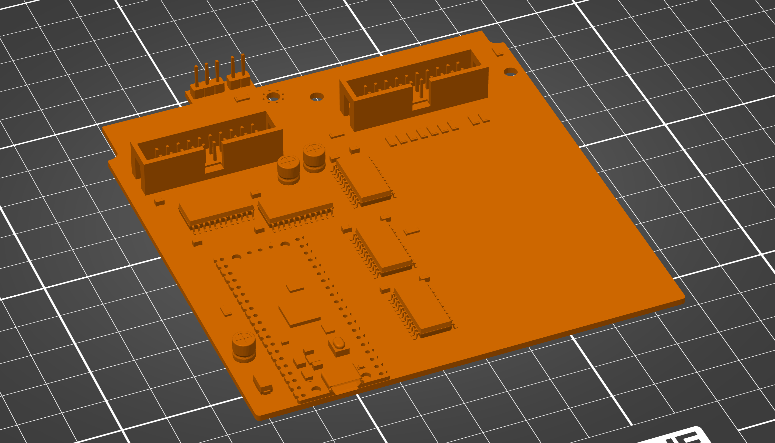
A STEP and an STL of the populated board came out of KiCad for a print, to check the parts against the inside of the UniDisk case the way the bare outline was checked in M7.1.
Open threads
- Rewire the prototype’s eight moved channels and check it still boots, before any order.
- The ground-plane slot between the headers: move one of the two power runs to the top layer, or live with it.
- Print the board and try it in the case.
- The measurements that need a ruler, not a bench: J4/J5 header pitch, J2/J3 positions on one more print, J1 pins-to-face, and the real front-panel eject cable’s pinout.