Disk Hamr: printed, fitted, ordered
The second layout got the same treatment as the first: print it, put it in the drive, see what hits. This time the print was made to be printable, the Gerbers went out the same morning, and the parts list got its last two corrections.
Print before fab
This board has been printed five times now. Each print is an hour of filament and it has paid for itself every time.
- Bare outline. The side mounting hole was too far down and too far from the edge.
- Outline again. Mounting holes fit.
- Outline with the DB-19 holes. The connector fit first try.
- First populated layout, from the KiCad STEP. The mechanism header sat too close and had to move 11 mm up toward the edge.
- This one, the second layout, the closest yet to the board that will come back from the fab.
The lesson came from Byte Hamr Rev 1. That board was right electrically and its USB connector kept the IIe lid from closing, so the card could only be programmed with the top off. A print of the populated board would have shown it in an afternoon; instead it waited for Rev 2. Since then every board gets printed with its parts on and tried in the thing it goes into before any Gerber leaves the machine. Collisions, connector reach, screw access, all of it shows up on the bench with a print, and none of it shows up in the 3D viewer.
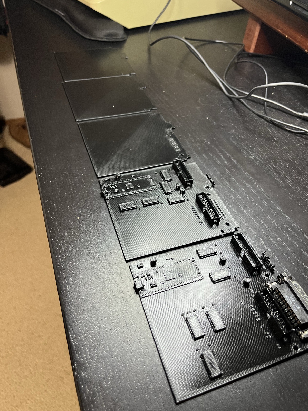
A print with nothing under it
KiCad’s STL export is honest to a fault. Every through-hole pin pokes 1.6 mm out of the bottom, every surface-mount part floats on the thickness of the copper the export leaves out, and the Pico’s USB jack is a hollow tin shell with 0.3 mm walls. Honest, and a mess to print: the pins want supports, the slicer flags every IC as an overhang, and the jack slices as a cavity.
So the mesh got a pass in Python with trimesh before the slicer saw it. Everything below the board’s bottom face is cut away and the cut capped, so the board sits flat on the bed. The board body is thickened to 1.86 mm, which swallows the 0.08 mm copper gap under every part and the 0.3 mm standoffs under the box headers and the SOICs. The USB jack is replaced by a solid block down to the bed. A ray walk through every footprint afterwards found no air between the board and any part. The slicer’s overhang view went from blue everywhere to blue on the electrolytic chamfers. No supports.
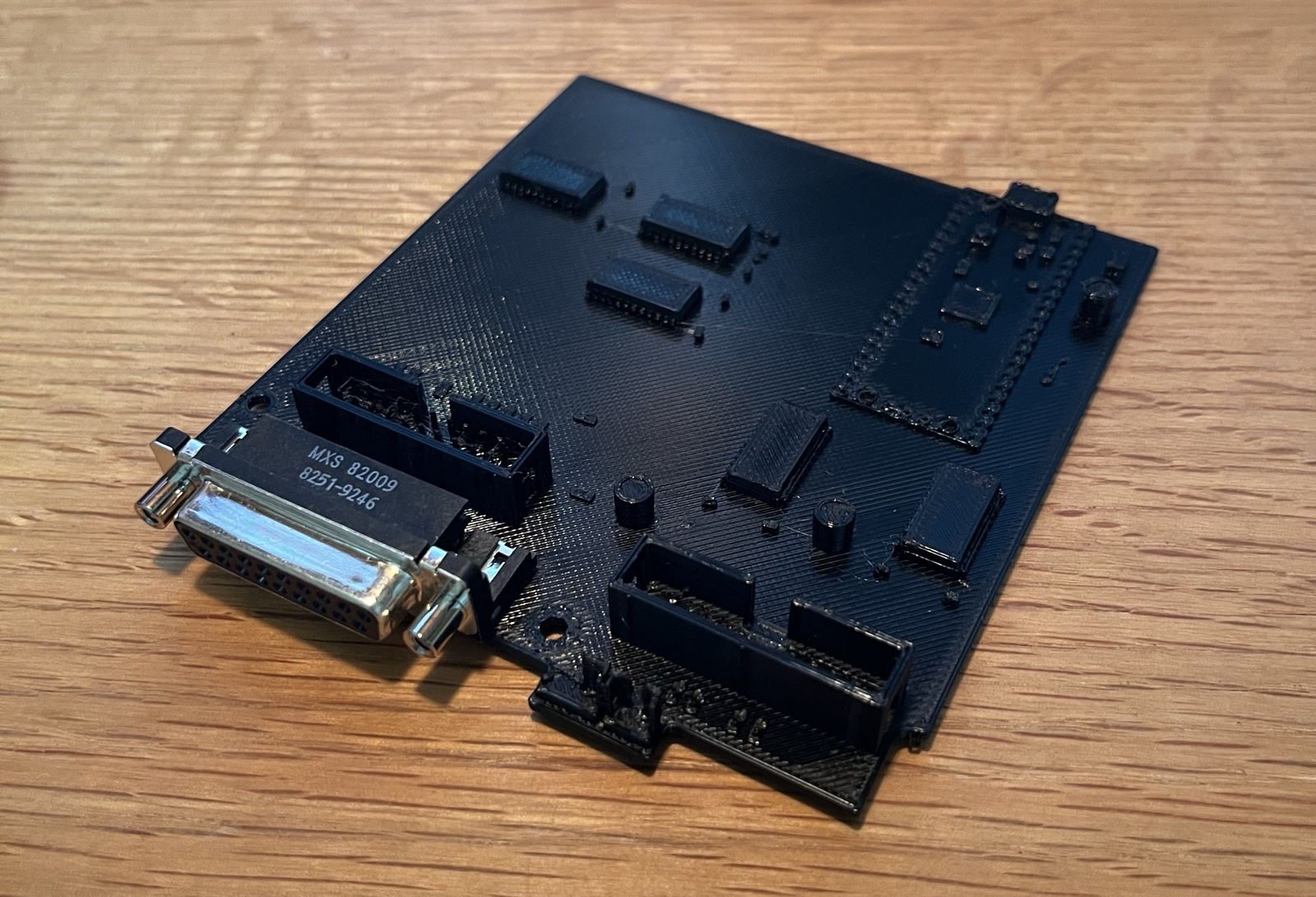
In the case
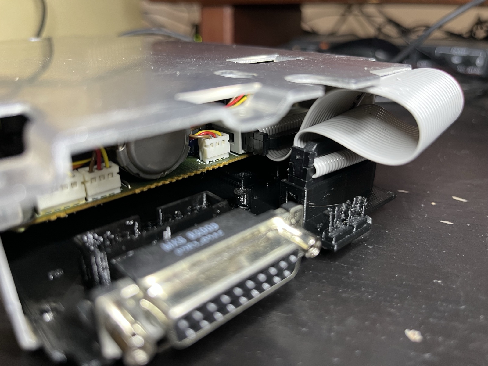
The print went in with the mechanism on top and the real DB-19 dropped into the printed holes. The mechanism’s 20-pin header, the reason for the second layout, is now where the ribbon wants it. The rear DB-19 sits in the case opening on the two M3 holes. The two tab headers for the LED and eject leads clear the lid.
To PCBWay
Gerber X2 and Excellon drills from KiCad 10.0.4, checked against the board before upload: 0.25 mm minimum track, 0.2 mm clearance, 0.3 mm minimum drill, and one via that had slipped to a 0.1 mm annular ring, which became a 1.0/0.5 mm Power-class via before the plot. Two layer, 1.6 mm, 1 oz, lead-free HASL, green, 6/6 mil, five boards. The only options worth touching on the order form were telling them where to put their product number (bottom side, away from the silk art) and ticking the free HASL-to-ENIG upgrade. A 0.12 mm stencil for the top side rides along with the order.
To DigiKey
The list is the bill of materials line for line, twelve DigiKey lines, about $20. Two things changed while checking it against stock.
The Yageo 2k pull-up for the rear port’s LASTONE line was out of stock until December; a Stackpole RMCF1206FT2K00 stands in. And the LED series resistor is settled: the original IF-83 pulls the LED anode to +5 V through 180 Ω, measured on the board, so R17 is 180 Ω too. Same current direction as the original, same brightness, about 17 mA from the shifter output, inside its rating. The parts list, schematic and board all say 180 now.
Not on DigiKey: the DB-19, the one rare part on the board and at $15 each from eBay the most expensive, already in hand and fit-tested.
How it will be built
Hot plate, stencil, paste, in one pass for every surface-mount part except the Pico: five SOIC-24 shifters, the 0805 decouplers, the 1206 pull-ups, the Schottky. Paste, place on the cold plate, check, power on, watch the joints go shiny, power off, leave it alone until solid. The board is 100 × 110 mm with a full ground plane on the back, so the plate’s heat spreads evenly, and with no top-side pour there are no pads sunk in copper to lag.
The Pico stays off the plate. On the plate it reaches reflow temperature and its own joints go liquid; nothing falls off, but that’s trusting it. It goes on afterwards: the paste on its 43 castellation pads gets wiped, the module seated, and each castellation ironed with a blob that wicks into the half-hole. Then the through-hole parts by iron: the two box headers, the two 2 mm tab headers, the three electrolytics, and the DB-19, tacked on one pin and squared to the case opening before the rest.
Waiting on
- The PCBWay boards, sponsorship or not.
- The DigiKey parts.
- Rewiring the prototype to the board’s shifter channel order and re-running the M9 checks before the boards land.