The sequencer that wasn't a computer
Backfilled from a post on embedded.greygiant.com dated 2025-07-16. The repo’s first commits are 2025-06-14.
What I tried
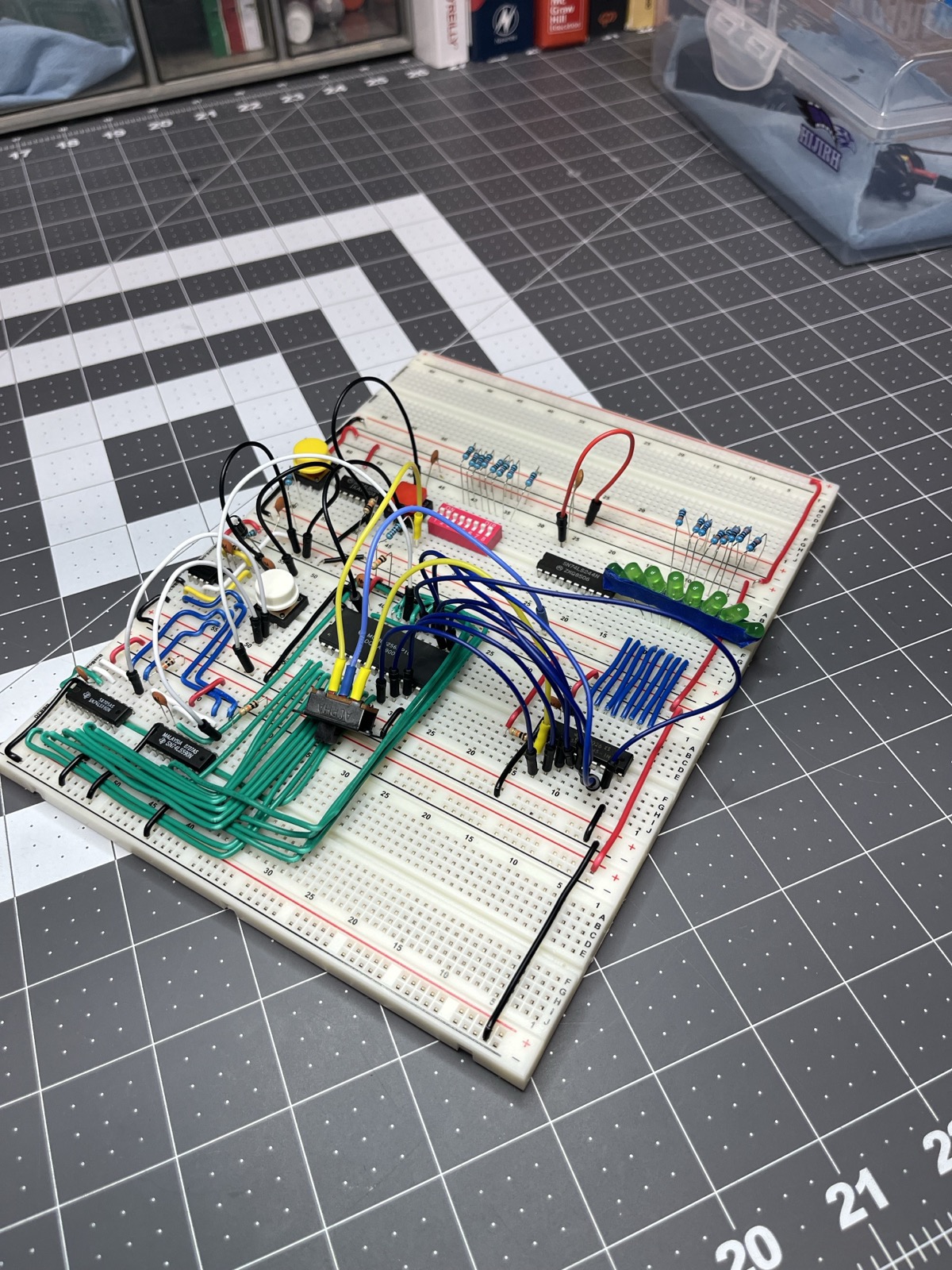
The first DINO was not a CPU. It was a sequencer. A 555 clocked two chained SN74LS590 8-bit counters into the address pins of an MCM60256AP-10 32K SRAM, and the SRAM’s data byte went out to eight LEDs. Two modes on a switch: LOAD lets you set a byte on a DIP switch and write it into the current address, RUN steps through the addresses and plays the bytes back. A 74LS645 transceiver sat between the DIP switch and the SRAM data pins. That’s the whole v0.0.1 schematic, dated 2025-06-15, which is the one on the project page under Hardware.
The plan on paper was a lot bigger than the board. 8-bit data, 16-bit address, 32K, a 74F382 for the ALU, and the thing it would eventually do was read a thermistor and drive a display and an analog output. I’d just come off bare-metal C on an RP2040 and wanted to know what’s underneath the microcontroller.
What I measured
The counter chain gave a clean 16-bit address. SRAM wrote and read back. I could key in a chase pattern on the DIP switch, store it, flip to RUN and watch it play. I wasn’t writing numbers down yet, so that’s all the record says.
What broke or surprised me
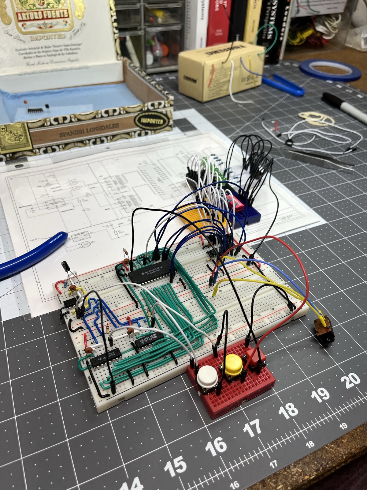
The moment three things shared the data bus (the switch, the SRAM, the LEDs) it fell apart. A DIP switch doesn’t make a logic level the SRAM is happy to write from. The ‘645 needed its direction and enable timed against the write, and the timing was whatever my finger did on the mode switch. And I couldn’t test the pieces one at a time, because checking the SRAM needed working bus control and checking bus control needed the SRAM.
What I had been calling “mode switching”, an AND gate and an SPDT, was the control unit. I didn’t have one. I went and read Malvino’s Digital Computer Electronics, the SAP-1 chapters. Control is a state machine with timed phases. Every enable is sequenced. Memory has setup and hold you have to meet. I’d been copying circuits that worked without knowing why they worked, and this was the first one that wouldn’t.
Next
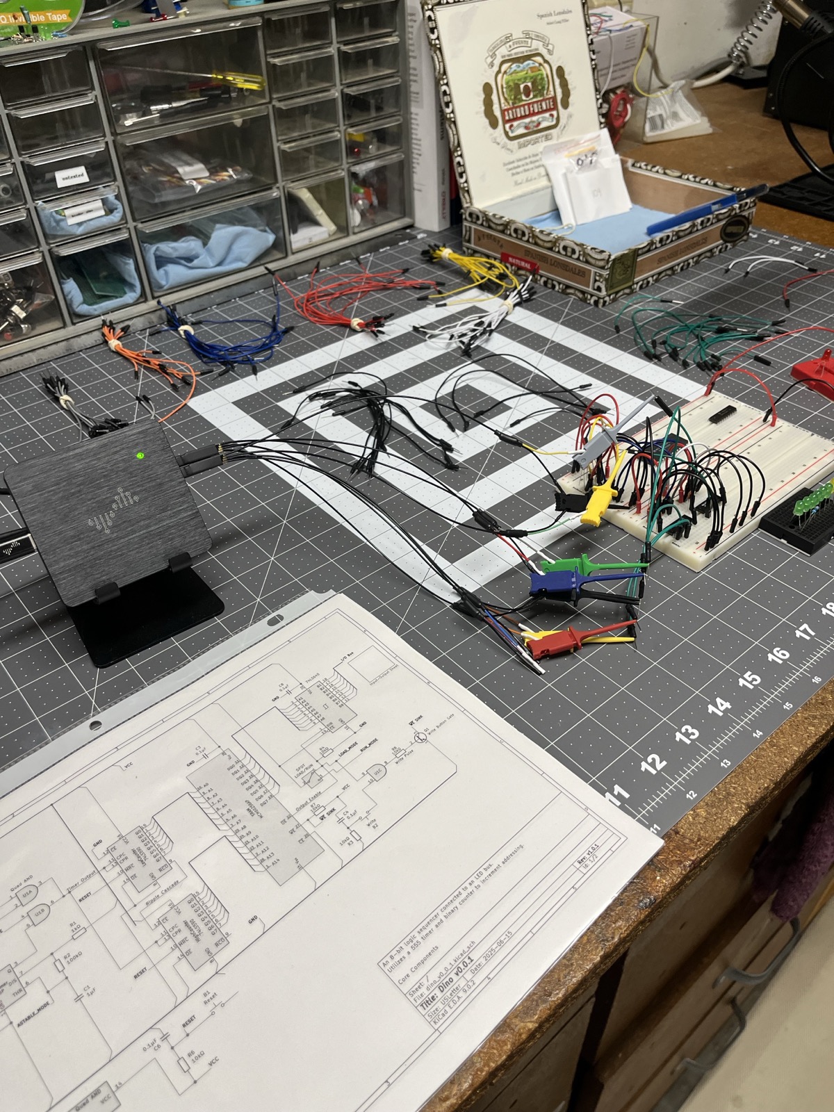
Keep the counter chain, the SRAM interface and the power and LED side. Read SAP-1 properly. Design the control word generation before touching wire again, and build modules that can be tested on their own.