The RET that fetched 0xFF was a 14 ns write
Three weeks of “a RET fetched from RAM reads 0xFF” ended today with one NOR gate and one inverter. The machine was writing its own RAM in the middle of a fetch. The write was 14 ns wide, it wrote the byte that was already there, and the SRAM’s read output came back wrong until the address changed. The IR latched 0xFF, which is HALT, and the machine stopped.
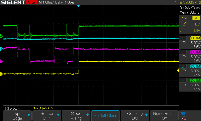
The gate that blocks it is in copper, in the KiCad, ERC clean, and beeped against the drawing. life.asm runs out of RAM for the first time and draws the Rule 30 triangle on the terminal until I hit Enter.
The bus was clean and the bridge was clean, so it had to be the chip
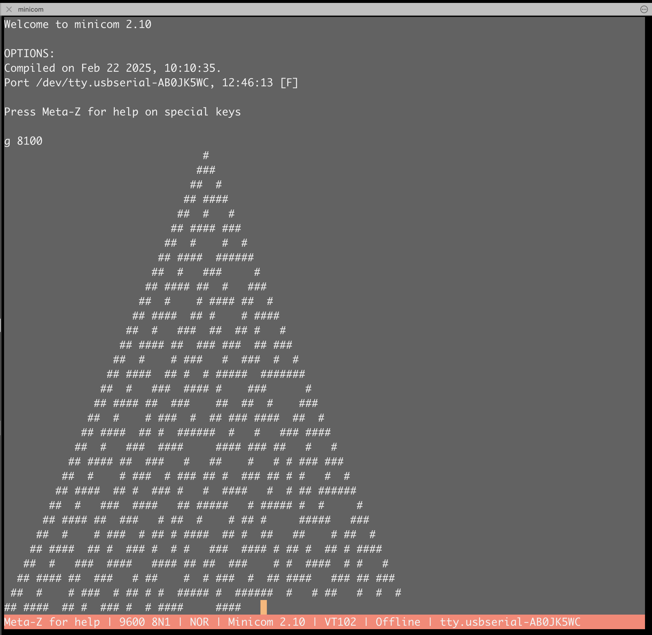
Yesterday’s capture showed IR bit 0 going to 1 about 60 ns into the RET fetch and staying there, with the address stable and the cell holding 0x34. The obvious suspect was the U25 bridge between the MDR bus and the W bus. Four probes on it: MDR0, the bridge enable, the bridge direction, HALT as the trigger. The bridge never let go and never turned round. The bad bit was already on MDR, driven hard, 16 ns edge to 5.3 V.
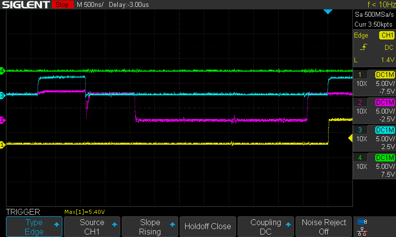
Next probe set moved to the RAM side of the ‘245 buffer. The SRAM’s own DQ0 pin went high 8 ns before MDR0 did. The ROM buffer’s enable never went low. So the SRAM itself was putting out a 1 from a cell that reads 0x34 afterwards, with its chip select low the whole time.
An SRAM does that in two cases. Either the address moved, or somebody wrote it. M0 held rock steady through the window on yesterday’s capture. That left the write.
~WE pulsed for 14 ns during the fetch
Probes on the SRAM’s ~WE (U26.27) and the ‘245’s direction pin (U21.1), 1 us/div, HALT trigger. The whole event is the single downward tick on the cyan trace, half a division left of the trigger marker, with a matching tick on green under it.
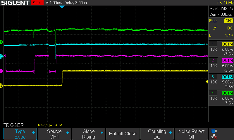
| signal | event, ns before HALT |
|---|---|
| ~WRITE_DIR (U21.1) | 16 ns low at -476 |
| ~WE (U26.27) | 14 ns low at -472 |
| RAM ~OE (U26.22) | 24 ns high at -466 |
| RAM DQ0 (U26.11) | goes 1 at -436, stays |
| MDR0 (U25.18) | goes 1 at -428, stays |
| LE_IR closes | -76 |
So in 30 ns the chip saw: write starts, output disabled, write ends, output enabled. The address was PC, 0x8103, and the data on the bus was the chip’s own 0x34, so the cell survived. What came out of the read path afterwards was a 1 on bit 0 and it stayed that way for 400 ns, until the PC incremented. I don’t have a datasheet sentence for what a 14 ns write pulse does to a 62256’s sense amps. The observation is that the output is undefined after one, at that address, until the next address change.
The same runt also wrote 0x00 into whatever address MAR held, at every RESET. I only noticed because I’d planted 0xA5 at 0x8200 as a sentinel and it kept reading 0x00 after each halt. That one happens at boot, during a fetch where the address mux also runts onto MAR for a few ns.
Where the runt comes from, and why ROM never cared
The write strobe is NAND(WRITE_DIR, ~CLK). WRITE_DIR is the DST decoder’s code 111 output, U30.7, through an inverter. The microcode EEPROMs are addressed by the IR and the T-count. In every execute row the IR is closed, so the EEPROM address only moves at CLK rise, and any decoder runt lands while CLK is high and the write gate is shut. That was the machine invariant and it held for 147 instructions from ROM.
The fetch row is the exception. The IR is transparent while CLK is low, the new opcode flows straight into the EEPROM address, and the ‘138 passes through code 111 for 14 to 16 ns on some transitions. The write gate is open at that moment. From ROM it never mattered because M15 is 0 and the SRAM isn’t selected; the runt hits a chip whose ~WE is tied high. From RAM the chip is selected and it takes the write.
That is also why the predecessor table from yesterday never made sense. Which instruction came before the RET decides which IR bits change, and which transitions cross 111. The same program has two RAM fetches, LDA then RET, and only one of them gets the write.
The fix is one NOR and one inverter
Every runt seen today is in T-state 0, the only state with the IR open, and no legit write ever happens in T-state 0. So the strobe is gated off there:
~RAM_WRITE_EN = NAND(WRITE_DIR, WR_GATE)
WR_GATE       = NOR(CLK, ~TO0)         U62 gate 4, a free '02 section
~TO0          = NOT(TO0)               U56 section 3->4, a free '14 section
TO0 is the one-hot T-state 0 off U7.15, active low. Six pins moved, three sheets touched, ERC 0, all six beeped good. ~IO_WR hangs off the same strobe, so the UART gets the same protection.
Witnesses, gate in:
| test | before | after |
|---|---|---|
| retlda (LDA 0x8200; RET) | halts 7 of 8 | 40 of 40 return |
| pulse trigger on ~WE, pulses under 59 ns | fires every run | never fires in 10 runs |
| step2, retmvi, retcrlf, callret, retinr, retldam, rethlsp | halted or mixed | 5 of 5 each |
| bigxfer, 2233 bytes | halted after the stream | returns to the prompt |
| 0xA5 planted at 0x8200, then a halt and a RESET | reads 0x00 | reads 0xA5 |
| life.asm | froze after row 0 on 09-08 | runs to the wall |
The wrong turns, in order
The first gate used the wrong signal. The handoff’s pin list said “T0 = U6.14” and I took it as the one-hot state. The netlist says U6.14 is the ‘163’s Q0, the count bit, and the one-hot is TO0 on U7.15. NOR(CLK, Q0) allowed writes only in even-numbered states and killed the monitor’s boot. An hour to find, and the rule about extracting from the netlist before naming a pin exists for exactly this.
A 100 pF went on the WRITE_DIR node on the theory that a ‘138 output into 100 pF would swallow a 16 ns runt. The node is driven by a ‘04, the runt did not move on the scope, and the cap came out for good. The halt rate did move while it was in, which is the reminder that a rate on this machine is not a measurement.
A pulse trigger sat on the RESET line for one batch while I thought it was on ~WE. That batch’s “no runt in 30 runs” is void and the record says so. Redone on the right pin.
Pulling that cap was followed by a power-down that left loose connections. For two hours after that the monitor halted at boot and sertx transmitted nothing. I found the wire, all but unplugged, seated it, and it all came back. During the same stretch I read “monitor halted” several times when the test ROM was in the socket, and test ROMs halt at their own end by design.
Two theories died on the scope. Removing a load from the ~CLK net did not change the edge at the flags register’s clock pin. And the delayed write strobe did not eat the UART’s data hold: sertx was silent with the gate in or out, because of the loose wires.
What’s still open
- Serial receive still loses 1 bits without the 22 pF on the UART’s A0 pin. With the gate in and the cap out,
sinstopfails four of four with the same 0x39 to 0x30 signature. The write runt was not the mechanism. The cap stays in. The planned capture is ~RD, M0 and CLK at the end of an RBR read, pattern trigger set at the panel. - One halt at PC 0x000x, once, mid serial payload. ROM bytes 0x0001 and 0x0004 are 0xFF operands, so a PC clear without a matching T clear lands there. RESET was not probed at the time. If it recurs the RESET probe goes on first.
- The interrupt images have never run. The halt blocked them. They are next when I say so.
- The OUT settle row burned into U15 on 09-08 fixes nothing and costs a T-state. Revert at the next burn, with the other 23 settle rows.
- Serial at 9600 8N1 was clean through the whole session with the cap in; the loader typed 2233 bytes into RAM and got them back with matching sums.