Rev 1.0 mainboard through PCBWay's audit
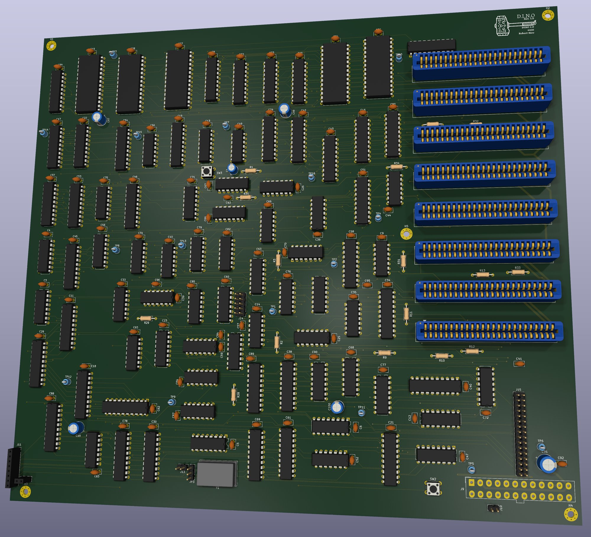
Five boards are through PCBWay’s audit, and the order goes in once shipping is sorted. 4 layers, 298.85 x 270 mm, 6/6 mil, 1.6 mm. KiCad DRC says 0 unconnected, 0 errors, schematic parity 0. The only warning left is the stroke weight on my TrueType board text.
| Board | |
|---|---|
| Size | 298.85 x 270 mm, 4 layers |
| Inner layers | GND plane, +5V plane, one piece each |
| Tracks | 0.2 mm minimum, 0.15 mm clearance; clocks 0.3/0.4, RESET 0.3/0.6 |
| Router | Freerouting 2.5.0, about 15 minutes from an empty board |
| Copper on the clocks | CLK 296 mm, ~CLK 283, CLK_B 162, CLK_ALU 48 |
Freerouting 2.1 would not join two pins next to each other
I let the router run all night on one placement after another. Every run stalled with a handful of connections left, somewhere between 3 and 20. Going through the leftovers, the same kind kept showing up: two pins on one chip, 2.54 mm apart, on the same net. U83 pins 3 and 4. U56 pins 9 and 10. Some nights U18 14/15 and U33 too. Freerouting 2.1.0 run headless never laid a track on them, on any placement, under the old rules or the new ones. I deleted just those two tracks from the board that had routed fine in the GUI before, and it couldn’t put them back either.
If your Freerouting run always stalls with a few unrouted connections between neighboring pins of one chip, try 2.5.0. It needs Java 25. It routed this board from empty to 0 unconnected in about 15 minutes, neighbors included, and finished on its own.
Two other things about 2.1 headless cost me most of the night. It ignores the pass limit, so a stalled run never writes its result. Setting a job timeout does make it write the board it has, unrouted connections and all, though now and then it hangs on the way out.
CLK_B could not fit between the socket pins
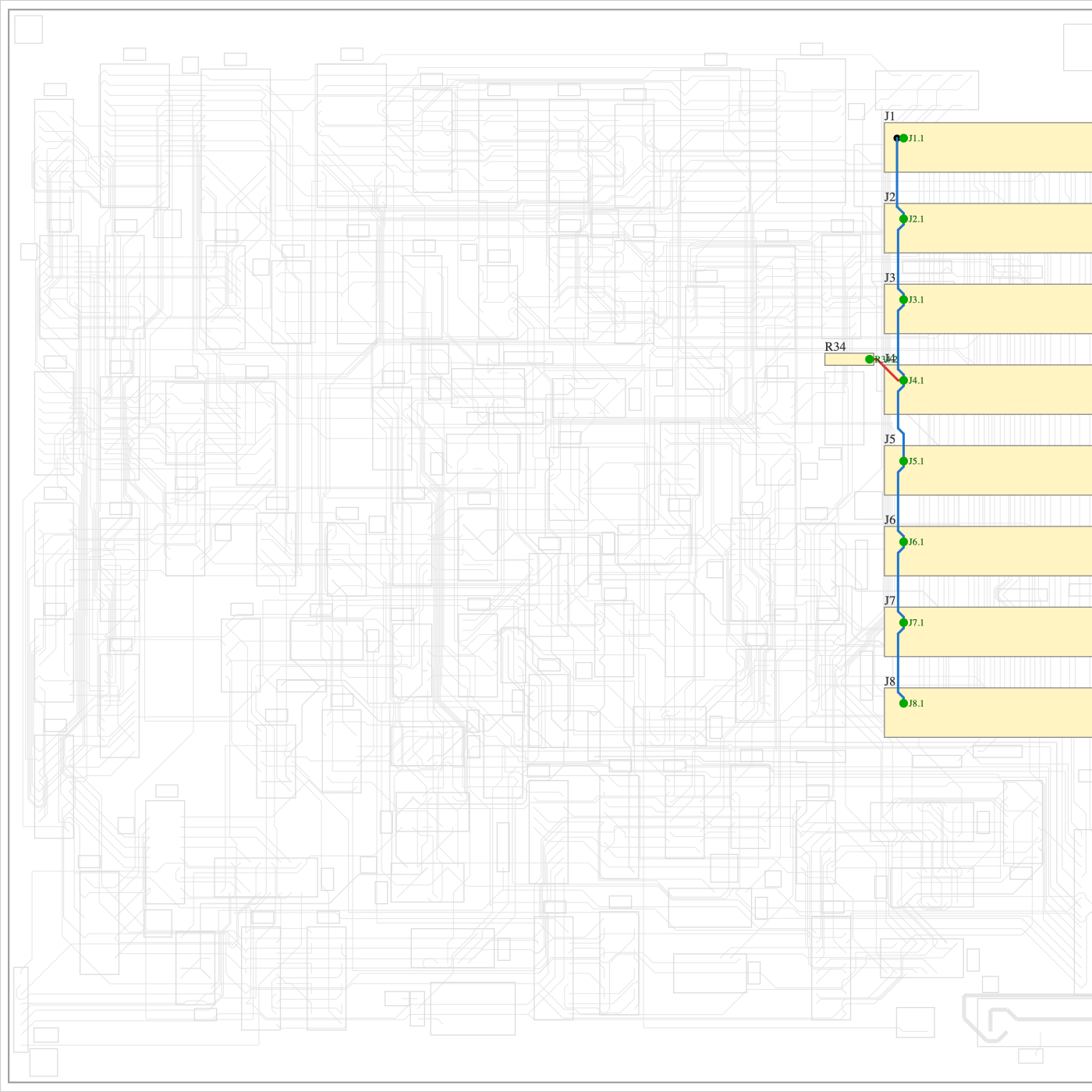
The card clock CLK_B was on edge pin 17, in the middle of a row. The pad gap on the Sullins socket is 0.84 mm. A CLK-class track needs 0.3 mm of copper plus 0.4 mm either side, so 1.1 mm. It couldn’t go between the pins of the other row, so every slot-to-slot hop went around the end of the row and back. That came to 517 mm of clock for about 200 mm of slot column.
I moved CLK_B to pin 1, at the end of the row, with +5V beside it and GND across from it. Now it runs straight down the column: 162 mm. No card exists yet, so the pinout change cost nothing. R34 (100 R) sits at the source, and Philips AN246 is the reason that matters: a source-terminated line only behaves while it’s electrically short.
Five reviews before ordering
Before uploading I had five separate reviews run over the fab package, power and signals, footprints, the schematic against the breadboard, and bring-up risk. The schematic one came back at 92/100. The core netlist is identical to the machine that ran BASIC on 10-06. Overall readiness came back at 72/100, and most of what dragged it down was debug access. The board had no test points, no logic analyzer header and no way to slow the clock or step it.
So the board picked up a batch before it went out:
| Change | Why |
|---|---|
| J14 clock select at U27.3: 1.024 MHz, 512k, 256k, 128k, or STEP from a debounced button (SW3 through a spare ‘14 section) | the breadboard’s speed jumper came back, plus single step |
| J15, 16 control signals with a GND pin beside each | the logic analyzer plugs straight in |
| 15 GND loops (Keystone 5006) and one +5V point | a short scope ground near every chip |
| U6 moved next to U27 | its clock pin was 138 mm out on raw CLK |
| C1/R1 moved onto U56 | the reset RC sat about 300 mm from the Schmitt input |
| Spare cap pads on CLK at U6.2, CLK_ALU at U47.11, HALT at U61.5 | somewhere to add back capacitance the breadboard had, without cutting tracks |
| Four 100 uF bulk caps spread out | |
| F1 removed | I don’t want a fuse on this board; the ATX supply has its own protection |
| Values: U56 SN7414N, U51 DM7400N, U36 74LS00, Y1 4.096 MHz | to match what’s actually on the bench |
I had test points backwards. I thought they were for seeing a signal. Every IC leg is already a signal point. What the board was missing was a ground for the scope probe close to where I’ll be probing, so the 15 cm clip lead stops ringing on a 5 ns edge. With 15 loops, 85 of the 87 ICs are within 50 mm of one.
Every clock and reset net, one at a time
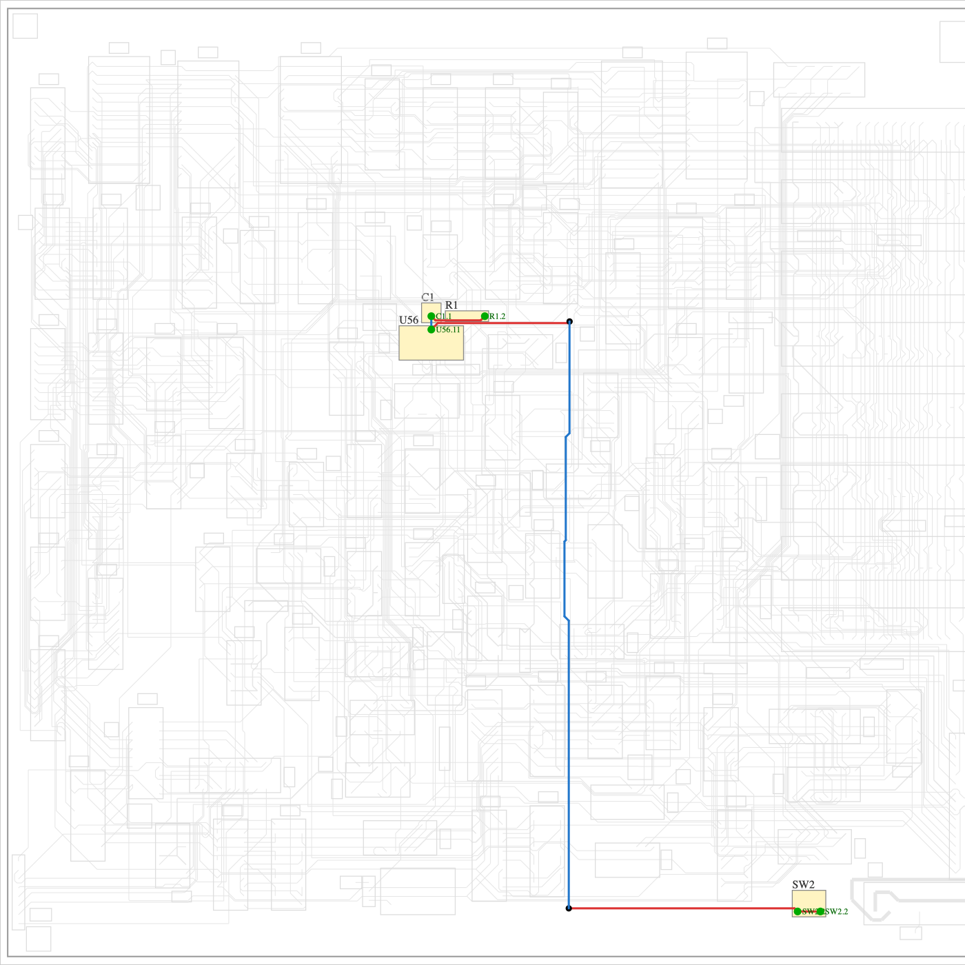
I drew each clock and reset net on its own over a faded board and went through them before ordering. Nothing needed re-routing.
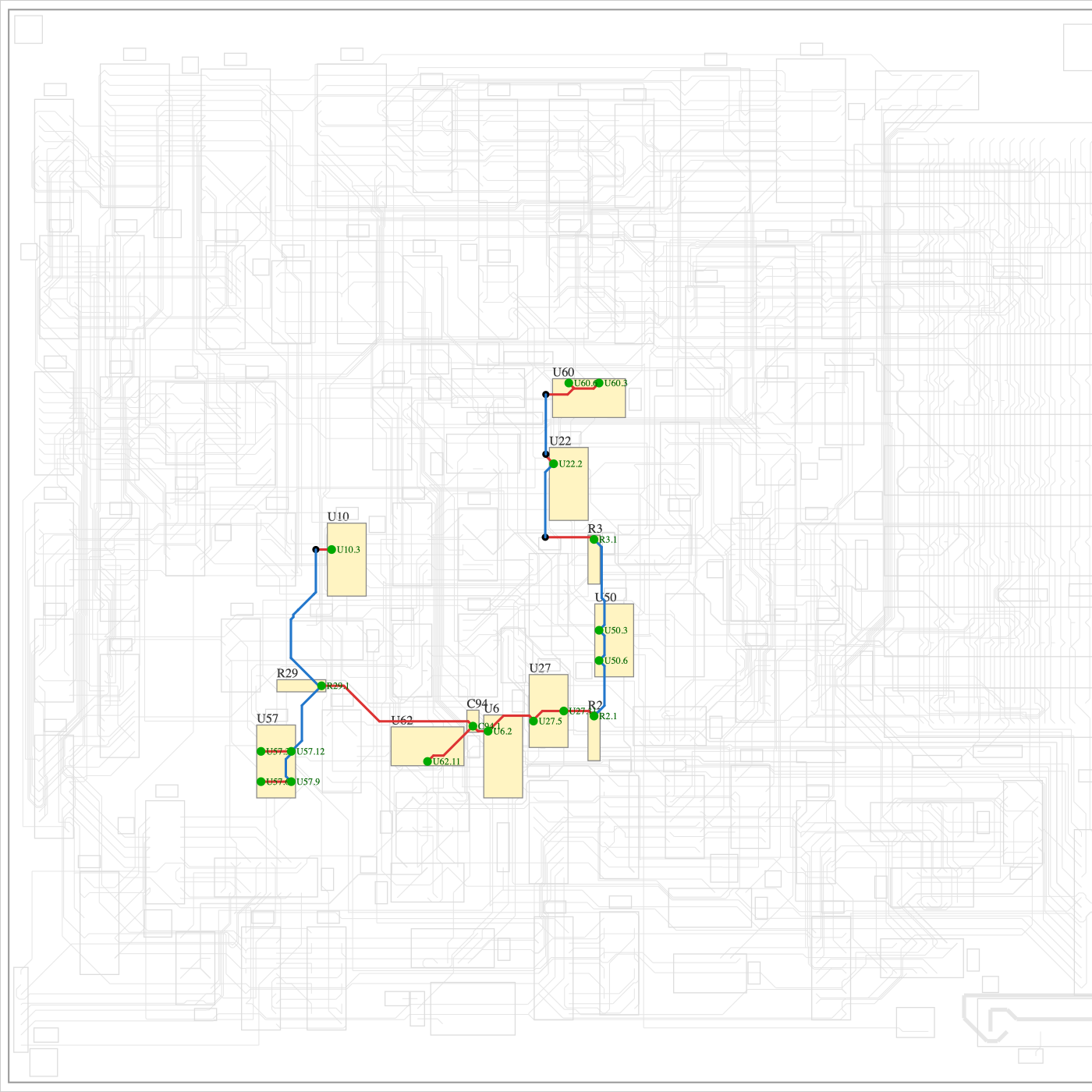
The one that looks wrong is the reset RC node. It’s 301 mm long and runs 50 mm beside M7. That run is the wire out to the reset button at the board edge. C1 (10 uF) sits right on U56.11, the only input on the net, so whatever the long run picks up has to go through 10 uF to get there. 5 pF of coupling against 10 uF is microvolts. I left it.
Open threads
- The ATX supply hasn’t been tested with DINO’s load on 5 V and nothing on 12 V. It’s an old group-regulated unit, so it may sit high or hiccup. That gets measured before the board powers up.
- No card plugs into a slot yet. The serial card has to move onto an edge card, either a wired Apple II proto card or one I draw. Watch the back row on an Apple card: Apple numbers it the other way round, so wire by position.
- The card schematic still has the old pinout with CLK_B on pin 17.
- No cap is on the ALU latch’s LE pin now, and the board has an empty pad there in case it wants one.
- Bring-up plan: bare board short check, clock and reset chips at a current limit, then everything with the probe ROM, then the coverage ROMs up to isa and isasoak, then the serial card.