A proto card for the slots
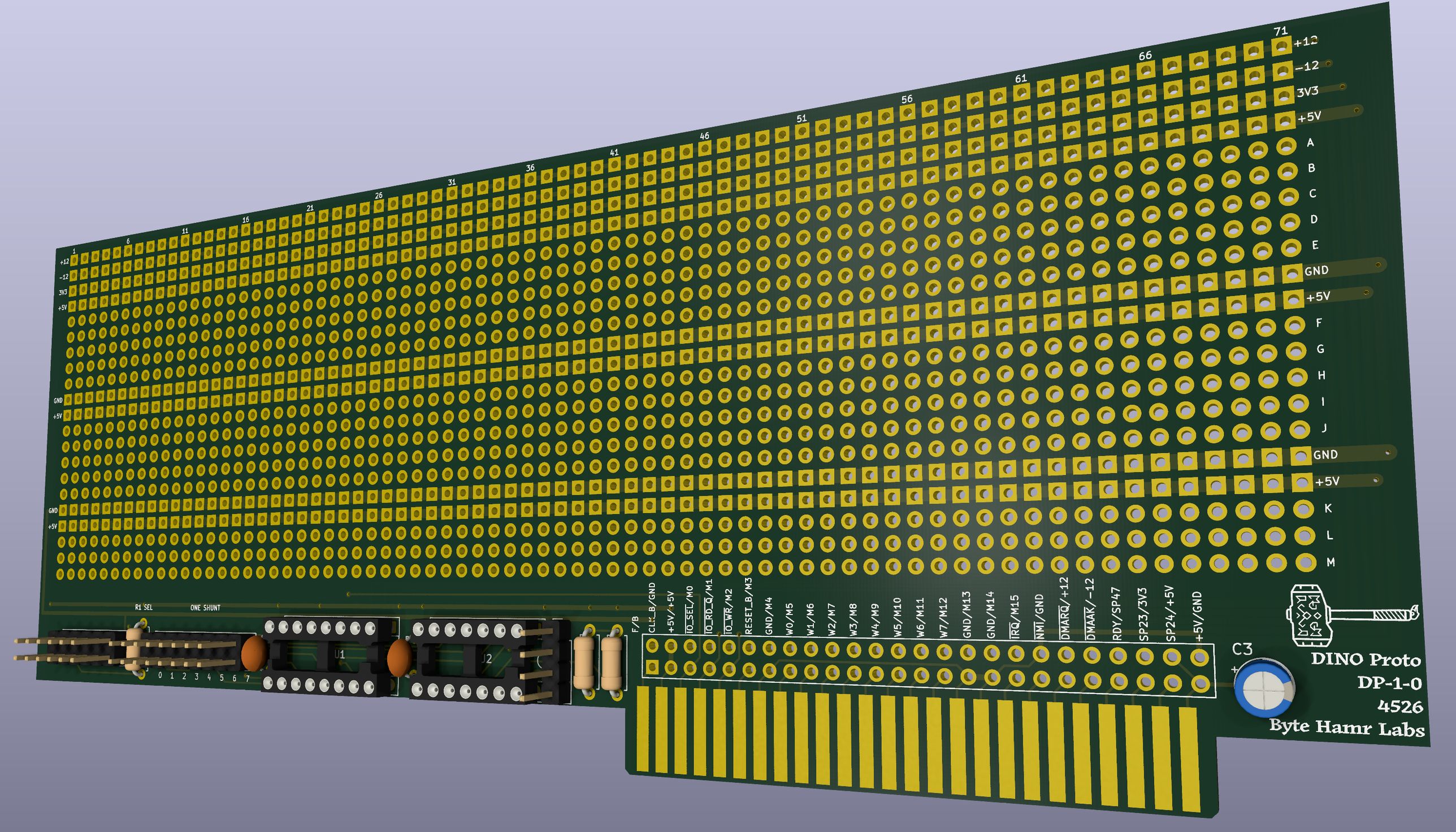
Rev 1.0 has eight card slots and nothing to plug into them. The serial card has no PCB, card zero has no PCB, and every card I want next (CompactFlash, a floppy hack, a front panel) is going to start as sockets and wire. So the first card is a prototype card: the part every card repeats in copper, and perfboard for the rest. If a bodge proves itself it can become its own board later, or never.
| Card | |
|---|---|
| Size | 191.8 x 70 mm body, 65.8 mm finger tab, 2 layers, 1.6 mm, all through-hole |
| Edge | 2x25 fingers, pin n opposite pin n+25, bevelled, gold |
| Fixed | ‘138 slot decode, 2x8 shunt header, ‘32 for the read and write strobes, a 2x25 bus breakout, 10 uF at the edge |
| Grid | 923 free holes, 71 columns by 13 rows, in three bands |
| Rails | +12V, -12V, +3.3V, then +5V / five free rows / GND, twice, as rows of square holes |
| Checks | DRC 0 errors, 0 warnings, schematic parity 0, ERC silent; 33 host tests |
What is fixed in copper
The ‘138 is wired exactly as the serial card’s: A0-A2 from M11-M13, enabled by ~IO_SEL. Its eight outputs land on the top row of a 2x8 header; the bottom row is all ~CARD_SEL, pulled up. One shunt in column n puts the card in slot n, 0x4000 plus 2K times n. Two shunts would short two totem-pole outputs together, so the rule is one, printed beside it. I went through a DIP switch with a diode per bit and a ‘151 mux with a 3-bit DIP before landing on the shunt: no extra chips, no diode drop on the select, and two shunts is a deliberate act in a way a flipped switch isn’t.
A 74LS32 makes ~CARD_RD (~CARD_SEL or ~IO_RD_Q) and ~CARD_WR (~CARD_SEL or ~IO_WR). Every card needs those two gates wired the same way, and getting them wrong is the classic card bug: a ‘244 enabled on the select alone drives W during the mainboard’s own cycles. One socket and 18 mm of board beats re-deriving it per bodge. The two spare gates come out on a 1x4.
J2 is the whole edge again as a 2x25 pin header, pin n = edge pin n, numbered by rows so it sits directly over the fingers with 2 mm tracks. A 50-way IDC ribbon off it is the bus on a breadboard.
Rails through the grid, not bars
An Apple II prototyping card I found on eBay for reference runs solid bars through its hole field, with rows of holes either side. What I didn’t want was signal copper under the chips, where you can’t see from one side what a pin is sitting on; a power rail under a chip, like the gap down the middle of a breadboard, would have been fine. What the card has is rail rows: one grid row of square plated holes, joined by a masked trace on both layers, with the round holes beside it free. Top to bottom: +12V, -12V, +3.3V, then a +5V row, five free rows, a GND row, twice over. A 0.3 inch DIP sits on rows 1 and 4 of a band with VCC and GND one row away; a 0.6 inch DIP spans into the next band, its body over the rails and no pin on them. Square against round so the eye tells a rail hole from a free one before a pin lands in it.
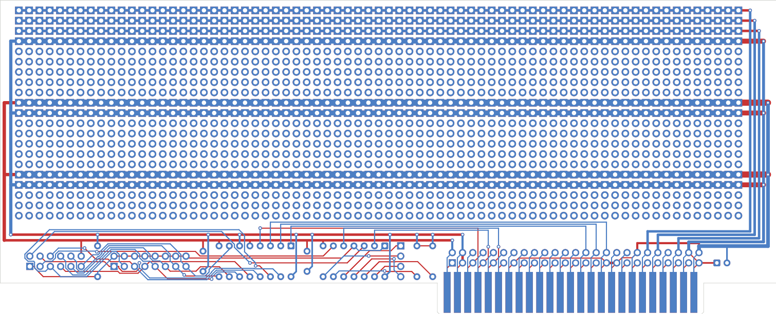
GND rows are 1.5 mm, +5V 1.2 mm, both layers. They’re fed from J2’s right end up the right margin with a via into each row, and tied together down the left margin, so each row is a loop fed from both ends rather than a stub; that was my addition after the first routed board came back with the rows dead-ended. The chips along the bottom get their own hole-less +5V and GND traces just above them. No ground plane: it’s a 2-layer perfboard and GND is a wire, which the breadboard already taught me. A 150 mA bodge drops about 10 mV across the card.
Generated, and what the router would not do
The card comes out of one script from the same bus table the mainboard’s sockets come from: the schematic with every pin on a global label, the project footprints (the rows-numbered header, the rail strips, the 923-hole grid), the outline with its chamfered tab, the placement, and the copper the card itself owns. The grid is a rule area; no track of the card’s may enter it, and DRC says so if one does.
Freerouting 2.4.1 does the band’s internal connections, about forty of them, pad to pad. It took five runs to learn what it will not do: connect to a track that was already there. The DSN marks pre-drawn copper as fixed wires, and the router completes a net only onto pads or its own wires. Every leftover, run after run, was a pad or wire that needed to land on one of my rails or feeds. So the generator draws every one of those joins itself, including a stub from each chip’s VCC and GND pin to its rail, computed from the real pad positions, and the six signals from J2 to the two chips as lanes between grid and band, ordered so no lane crosses another’s drop. The router gets only signals, and finishes.
It also routes straight through a perfboard until told the holes are a keep-out; a no-net pad is free space to it.
Overhang
The card sits with its tab in the socket and the body hanging left over the mainboard, Apple II style. The rule from the start was no more than 20 mm past the tab’s right end, where a case wall will be one day. The first cut was a Byte Hamr-sized 97 mm card; the second was 177.8 mm and measured 20.23 past the tab. This one is 18 past, 108 to the left.
Gerbers are out for a quote. Before an order: the Sullins socket’s slot opening against the 65.8 mm tab, which I still haven’t measured. The one DRC item left is the stroke weight on my own TrueType title text, same as Rev 1.0.