No DMA on DINO
DINO isn’t getting DMA. It goes to the next machine, which will probably be 16-bit and probably built around a real CPU instead of TTL. This one goes to PCB, then gets a CF card and a floppy card. I got there by finally working out where the DMA hardware would physically live on the breadboard, and then by asking what I wanted it for.
Where the DMA chips would have gone
The KiCad sheets don’t tell you which breadboard a chip is on. That has bitten me before, so I marked up photos of the bench chip by chip instead.
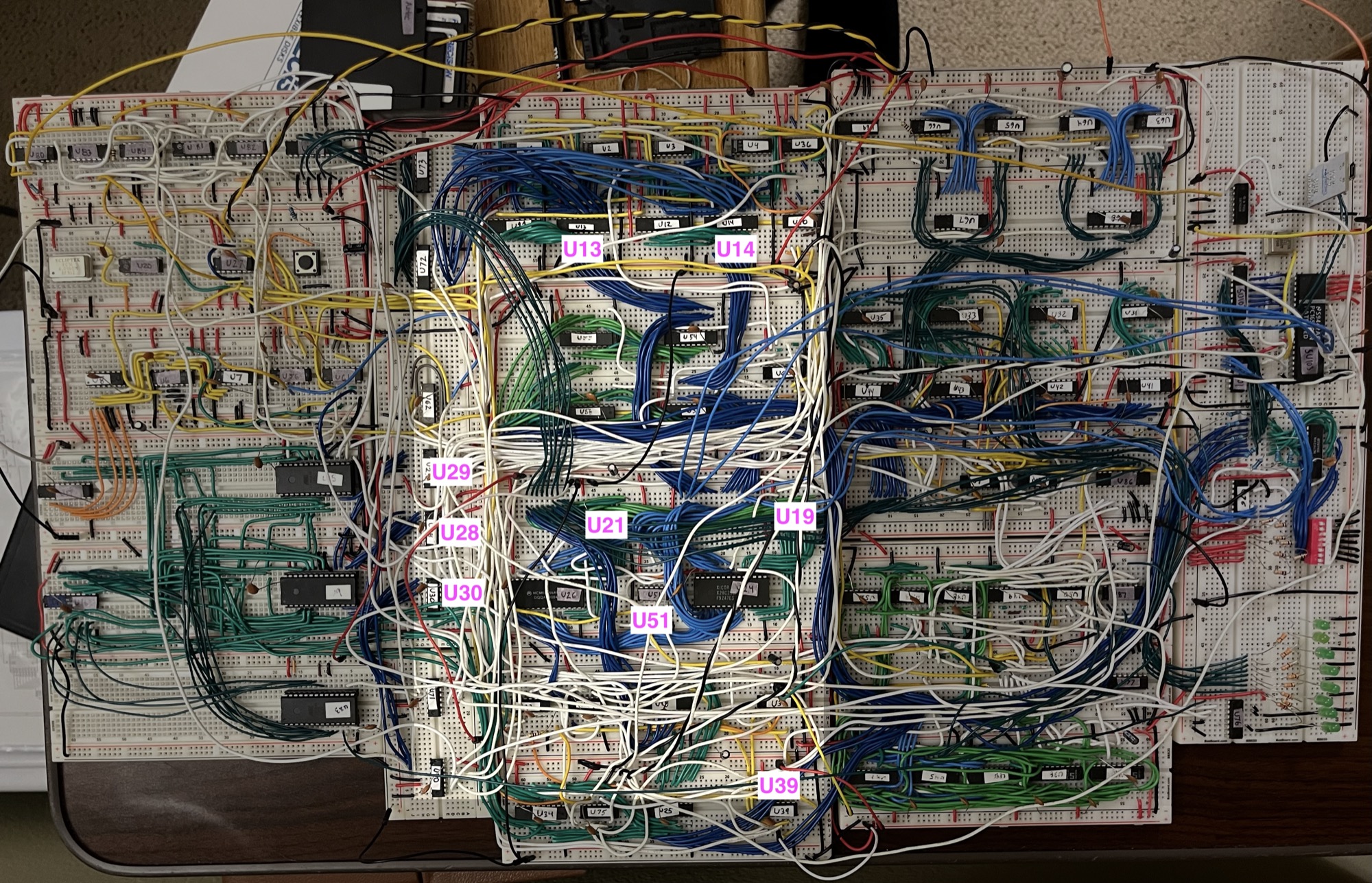
Most of it clusters on or next to the center board, where the MAR drivers, the RAM and ROM, and the M bus all are. The interrupt chips are the exception, up in the top left corner with the clock and reset.
| Item | Count |
|---|---|
| Existing pins lifted | 20, on 16 chips |
| New ICs | 13 (4 for the core hooks, 9 for the 8257 and its buffers) |
| Passives | about 25 |
| Full-size breadboards for all of it | 3 |
| Wires between the old boards and the new ones | about 60 |
| Long runs, to the interrupt board | 5 |
There’s no room left on the existing boards, so all 13 chips would go on a second floor over the center board. The best mount I came up with was a C-shaped shelf, with a long lower leg underneath and the top shelf over the center board. The shelf would also cover 7 of the 20 pins I’d be rewiring.
One thing I didn’t know: the clock buffer for the card slots, U78, only exists on the PCB. The breadboard has no edge connectors, so DMA would have needed its own clock inverter anyway.
Where the registers would have lived
I’d settled on 0x7800, the top 2K of the I/O window, with its own decode. I tried to reuse the ‘138 on the DIP switch card, but its outputs only fire on reads, and the 8257 needs writes too. ROM space has no write strobe at all.
What I want DMA for is a floppy
I have an old 3.5" PC floppy drive and a couple of IDE drives. IDE drives buffer the whole sector and wait for the CPU, so they don’t need DMA. CF in PIO mode is the same. The floppy is the only one that can’t wait.
I worked out the timing from the microcode’s T-state counts. A T-state is about 1 us at 1.024 MHz. The loops are sketched, not assembled.
| Way of reading the floppy | Per byte | 720K (byte every 32 us) | 1.44M (byte every 16 us) |
|---|---|---|---|
| Poll the controller’s status, then read and store | ~30 us | no margin | too slow |
| CPU stalls on RDY until the byte is ready, normal loop | ~18 us | fits | too slow |
| Stall on RDY, loop unrolled 512 times in RAM | ~10 us | fits | fits |
| DMA | ~1-2 us | fits | fits |
So the floppy needs help from somewhere. Earlier today I asked whether a Z84C10 would be easier than the 8257. It saves 2 or 3 chips on DINO, mostly because it drives the address bus itself. The core hooks stay the same either way, and those were what worried me.
The 8257 itself didn’t worry me, since it’s a real chip that works. Cutting 20 working pins on a homemade CPU to bolt on bus mastering it was never designed for did.
Rev A
The floppy card will handle its own timing. The core doesn’t honor RDY, but RDY gets a pull-up on Rev A, and the edge connector keeps the DMA request, acknowledge and RDY pins. On DINO2, bus mastering goes in from the first schematic.
Disappointed, but it’s the right call
I’m disappointed. DMA was the last thing on the list for this machine, and I’ve gone back and forth on it since September. I think dropping it is the best call anyway. Once the PCB runs the same setup the breadboard does, I get a mountain of wires and breadboards back, and that’s where DINO2 starts.
Open
- The PCB is placed but not routed. Freerouting does the routing. I’ll place the chips myself, since I place better than Konnect does, or let Konnect place them and do no routing.
- Power comes from an old ATX tower supply. The connector and the power routing on the board are next.
- The RDY pull-up still has to be drawn.
- The floppy card: which controller, and how it buffers a sector.
- The CF card is 8-bit only. A spinning IDE drive needs the 16-bit latch pair added.