Microcode decoder: two AT28C64s and four '138s
Backfilled from a post on embedded.greygiant.com dated 2025-08-11.
What I tried
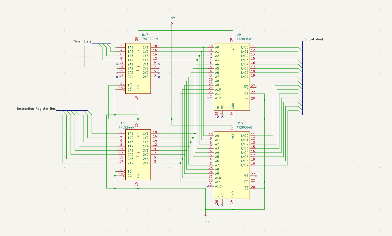
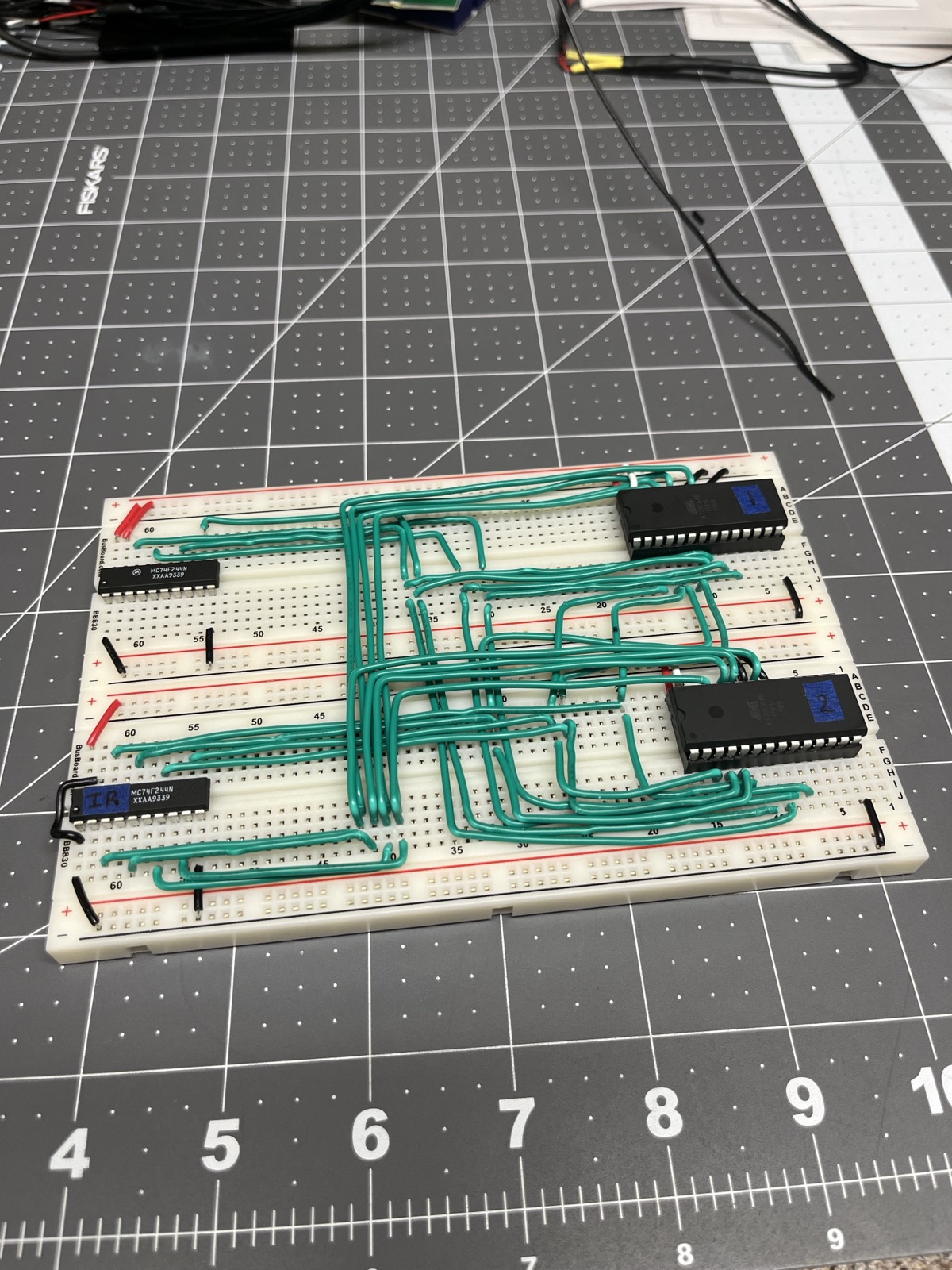
The control word generator as its own module. The timer state from the ring counter and the opcode from the IR go in as an address; two AT28C64 EEPROMs in parallel give a 16-bit word back, ROM 1 the high byte and ROM 2 the low byte. Four 74LS138s split twelve of the bits into the banks worked out in July, and four bits go straight out for signals that aren’t mutually exclusive with anything.
![The four '138 decoder banks on the control word: ALU ops on [11:9], PC and system control on [8:6], memory ops on [5:3], register ops on [2:0]. PULSE_REQ, PC_UP, PC_MAR_MUX and HALT are direct bits.](/img/dino/2025-08-11-decoder-banks-schematic.png)
The instruction set at this point: LDAI, LDBI, STA, STB, NOP, LDA, ADD, MOV, OUT, HLT. Enough to exercise memory both ways, the registers, one ALU op and the output.
Control word changes since July: bit 13 became PC_UP, bit 12 became PULSE_REQ, IR_LOAD moved into the ALU bank as code 111, and MDR_OUT, OUT_REG_LOAD and OUT_REG_OUT got slots in banks 3 and 2.
Two things I got wrong on paper
- I’d written the whole ISA with the first bit as MSB and the hardware wanted it as LSB. Redrew the schematic. The address into the ROM is opcode and timer state side by side, so once the order was right you can read the microcode address straight off the IR.
- Some latches can’t be trusted to close on a full T-phase. If HALT and a latch enable land in the same phase there’s no telling whether the latch captured stable data. So PULSE_REQ: a 74LS121 one-shot fires partway into the phase, early enough that the bus has settled, and RAM writes and ‘373 loads key off that pulse instead of the phase level.
Boot
Microcode addresses 0x0000 to 0x000F are the boot sequence. In reset, a 74LS244 with its inputs tied to ground forces opcode 0x00 onto the IR bus and a 74LS73 JK flip-flop holds it there until reset is released. Row 0 clears the PC, row 0x0F increments it, and the IR only starts loading real opcodes after reset lets go.
What I measured
Test image, not real microcode: 0xDEAD at 0x0000, 0xBEEF at 0x0001, 0xBEEF at 0x0DED, 0xFEED at 0x0FED, everything else zero. A little C program writes the two .bin files, another reads them back and prints the bytes at those addresses so the burn can be checked against the file.
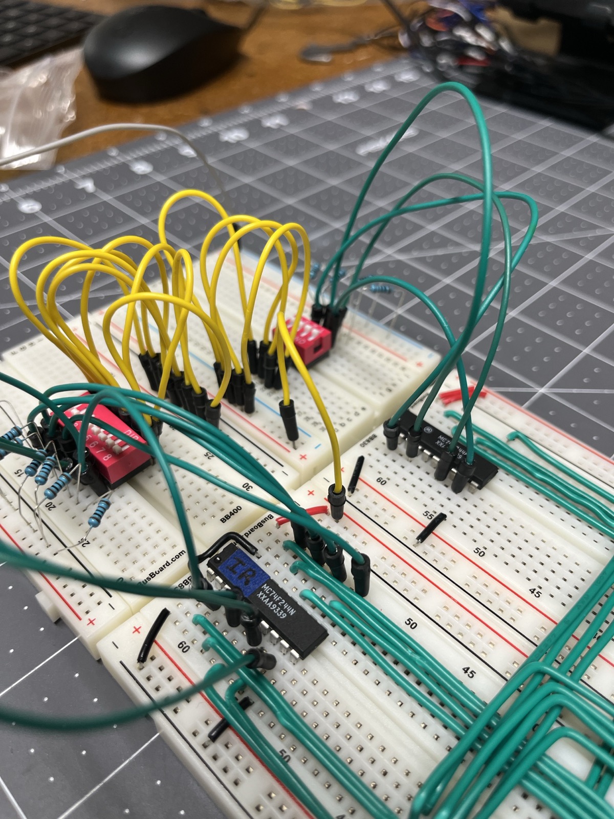
Two 8-way DIP switches set the address. A multimeter on each of the sixteen output pins, written into the journal, converted to hex, compared to the file. With the address static the LA had nothing to add. Burned with a T48 over minipro.
0x0000   DE AD
0x0001   BE EF
0x0DED   BE EF
0x0FED   FE ED
Took several rewire and re-burn rounds before all four matched.
Also drawn
The MDR, IR, memory and register sheets are all in KiCad now, before any of them is wired, so the datapath is consistent on paper first.
Next
MDR, then IR, then the memory module and registers.