Memory module: the SRAM wants an edge on WE
Backfilled from a post on embedded.greygiant.com dated 2025-08-19.
What I tried
The memory board: a 28C256 as 32K program ROM, the MCM60256 as 32K RAM, both on the 16-bit address bus, each through a 74LS245 onto the 8-bit data bus with eight LEDs on it so I can see what’s there. The ROM’s ‘245 has DIR tied for output only and its enable on ROM_OUT. The RAM’s ‘245 gets DIR from RAM_LOAD and RAM_OUT so it goes both ways. Only one is ever enabled.
The first drawing had a 74LS244 on the ROM side. Swapping it for a ‘245 made the two sides the same footprint and pinout, and the ‘245 drives harder anyway.
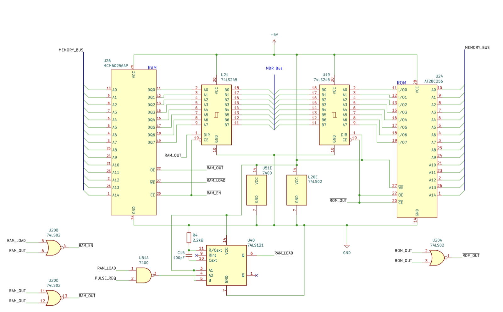
Four control bits from the decoder board drive it: ROM_OUT and RAM_OUT from bank 2, RAM_LOAD from bank 2, and PULSE_REQ on bit 12.
What broke
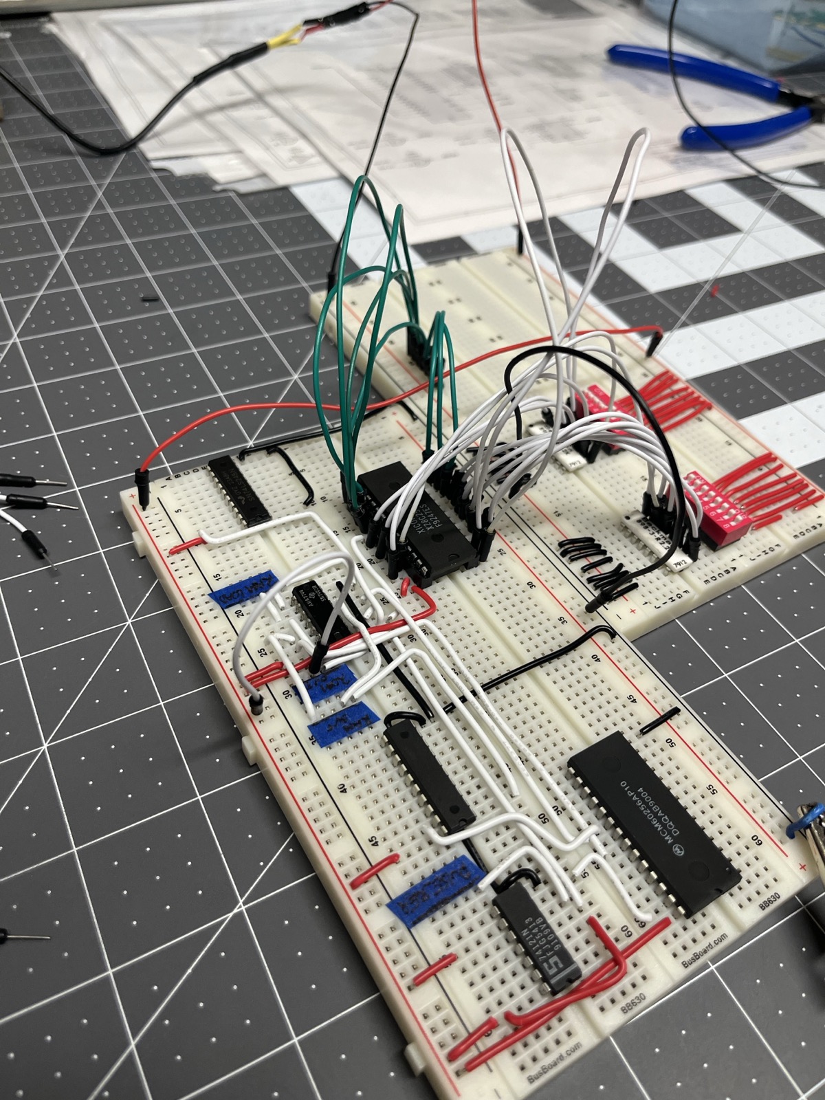
- Bit order. The binary patterns coming out didn’t match the file. I’d had the data pins backwards: I/O7 on the RAM and the ROM was landing on the bus as the LSB. Rewired the whole data interface so the bus reads the same on every board.
- Writes. Holding WE low for a T-phase did not write the SRAM. It wants an edge. So the 74LS121 got a job: a 600 ns active-low pulse, triggered with the other control bits, that gives the bus time to settle and then gives the SRAM a clean falling edge and is back high before the next phase. t = 0.7 RC, 10k, 86 pF for 600 ns, 100 pF fitted. Both A1 and B on the ‘121 needed pull-ups; feeding PULSE_REQ straight into B was intermittent. The NOR I first used to trigger it wasn’t deterministic either and became a NAND.
This ‘121 didn’t survive into the machine that runs today. RAM write is clock-qualified now and there’s no one-shot anywhere, which is why the clock can stop.
How it was tested
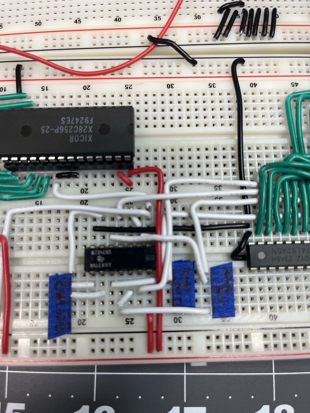
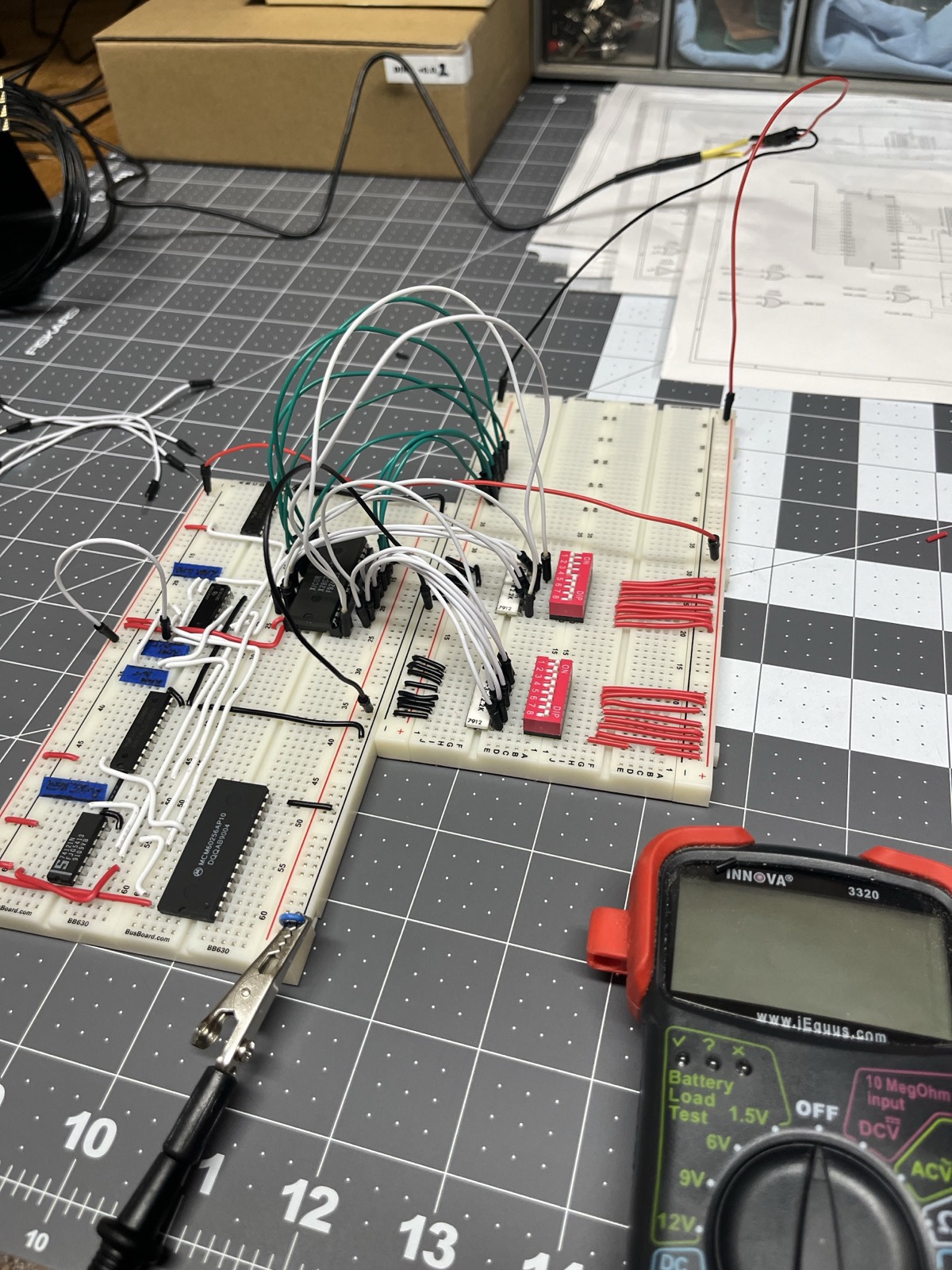
Two 8-way DIP switches with Beckman 3.3k pull-down arrays set the address. Eight LEDs through 220R show the data bus.
Two C programs. One fills the program ROM with test bytes: 0xAA at 0x0000, 0x55 at 0x0001, 0x12 at 0x1234, 0xCD at 0xABCD. The other writes a test ROM that acts as a tiny microcode controller for the RAM: it puts a byte on the bus, asserts RAM_LOAD and PULSE_REQ in the same word, then asserts RAM_OUT to read it back. All the control bits land at once, the way the real decoder will drive them, instead of me flipping switches with skew between them.
What I measured
- ROM_OUT: the LEDs show the burned byte at each test address.
- PULSE_REQ: scope on the ‘121 output, 600 ns wide, clean edges.
- RAM_LOAD with PULSE_REQ: byte lands in the SRAM.
- RAM_OUT at the same address: the byte comes back.
One dead end on the way. I tried to share the address generator between the test ROM’s own reads and the SRAM under test, wrote to one address and read garbage from another. Separate addresses per phase fixed it. Trying to move too fast.
Next
The MDR, the latch between memory and the registers. Three schematic revisions on this board; I expect the same on that one.