Four layers, DMA dropped again, interrupts on a branch
The board is 4 layers now, DMA came off the plan (again, maybe not for good), and interrupts exist as microcode on a git branch that nothing has run yet. Then I put DINO back on the shelf. It started to feel like work somewhere in these two days, and I’d rather come back to it when I want to.
Four layers cost $70 more than two
I got PCBWay quotes for 5 boards, 298.85 x 222.8 mm, 1.6 mm FR-4, 6/6 mil, 0.3 mm minimum hole, HASL lead-free, DHL to the US.
| layers | PCB | total with shipping |
|---|---|---|
| 2 | $109.49 (24 h build) | $142.96 |
| 4 | $181.20 (4-5 day build) | $212.51 |
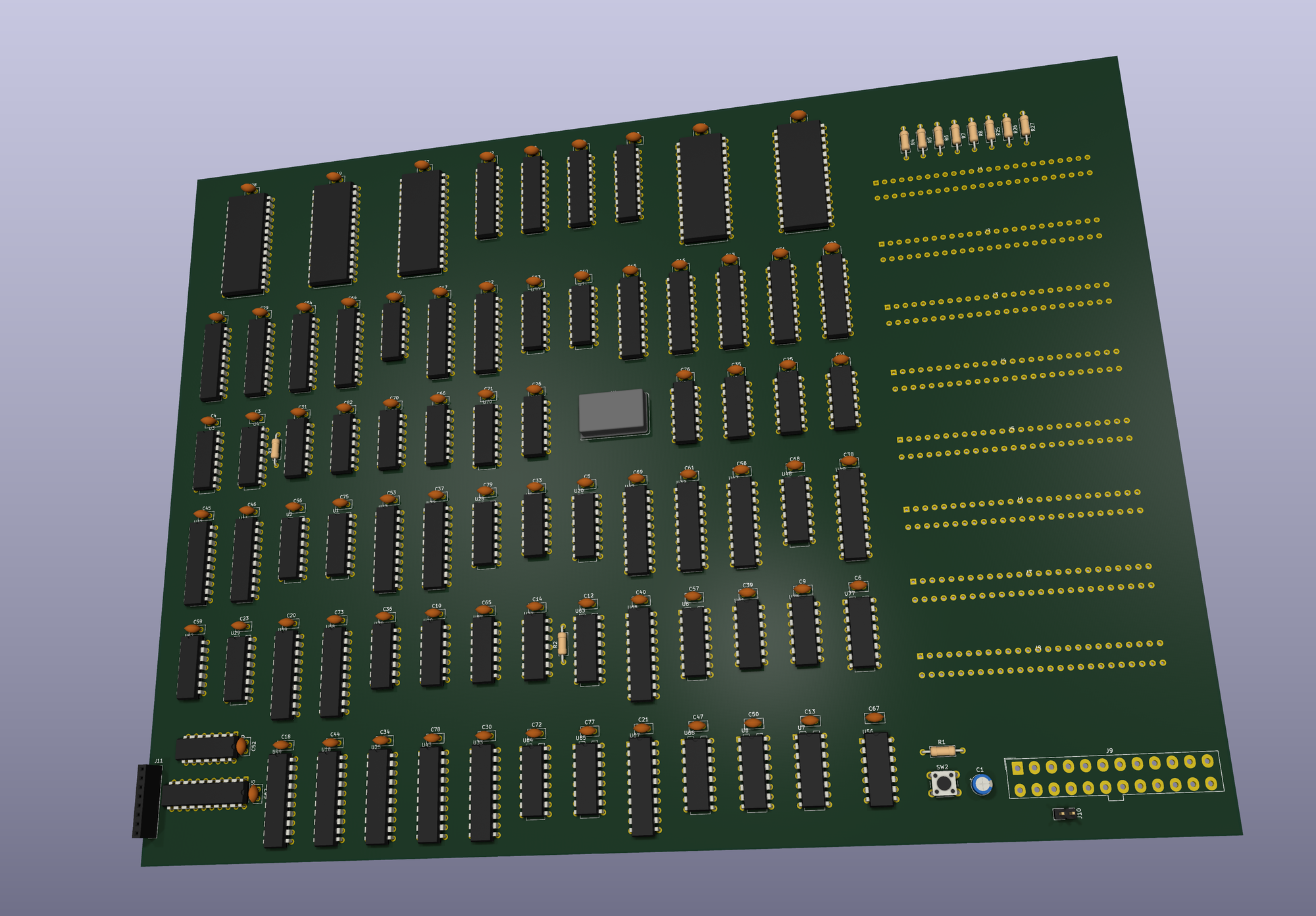
The autorouted 2-layer board had a GND pour that was really a mesh. The pour alone stranded 67 pads, and B.Cu carried 3617 mm of ground as tracks. The worst weeks on this machine were ground offset and pickup, so $70 was an easy call. I deleted every track, via and zone, kept the placement, and laid In1.Cu as a GND plane and In2.Cu as a +5V plane. DRC says GND and +5V reach every pad through the planes, and 499 signal connections are left for the reroute. The old 2-layer route is still in the repo history if I ever want it.
A free ATX supply and a case I don’t have to design
I have a spare Foxconn HH-400UNEA (ATX12V 2.2, Delta-built) off an old PC.
| rail | rating |
|---|---|
| +5V | 21 A |
| +3.3V | 18 A |
| +12V | 11 A + 15 A, 19 A combined |
| -12V | 0.3 A |
| +5VSB | 2.5 A |
| -5V | none |
DINO draws 1.25 to 1.34 A. The Foxconn plugs into the same 24-pin J9 as a picoPSU, so the board doesn’t care which one I pick, and I haven’t picked yet. Nothing on the machine needs -5V, so there won’t be any. RS-232 can come from a MAX232 or from a 1488 running off the ±12V the card slots already carry.
I looked at making the mainboard ATX so an old PC case would do. The outline fits inside 305 x 244 mm and the slots are already on 0.8 inch pitch, but they run along the short edge, there are 8 of them, and the cards aren’t PCI, so the case brackets would never line up. A wood or 3D printed case is less work. The board has no mounting holes yet, which it needs whatever the case is.
DMA came off the plan again
I went into this thinking DMA was a handful of chips. The breadboard BOM came to 12 on the core (8257, ‘244, ‘373, two ‘245s, two HCT'157s, ‘74, ‘08, ‘32, ‘04, ‘138) plus 2 on the serial card. Most of that count is the bus. DINO was built so only the CPU ever drives the address bus or the RAM strobes. The M drivers are two ‘245 pairs with complementary enables, so M never floats, and the RAM strobes are push-pull gate outputs. Every one of those needs a mux to hand it over, and the NMOS 8257 can only sink 1.6 mA, so it needs buffers to drive an LS bus at all.
The only thing on the roadmap it would speed up is loading from CompactFlash, about 256 KB/s against 33 KB/s polled. All of RAM is 32K, so polling fills it in about a second. Right now that doesn’t feel worth a dozen chips.
This is the second time DMA has been dropped. Byte Hamr on the Apple II doesn’t have it either, because the address bus there is unidirectional. Both times it came down to how the bus was built. If I want bus mastering on the next machine, the address bus and memory strobes have to be tri-stateable in the first schematic, when it costs nothing.
Interrupts are written and tested on the host only
| opcode | instruction |
|---|---|
| 0x90 | INT (injected by hardware, the assemblers refuse it) |
| 0x91 | IRET |
| 0x92 | EI |
| 0x93 | DI |
| 0x94 | PUSHF |
| 0x95 | POPF |
When an interrupt is accepted at the end of an instruction (or in HALT), the hardware holds the ROM and RAM buffers off for one fetch, a ‘244 puts 0x90 on MDR, and the PC doesn’t count. So IR gets INT and the PC still points at the instruction that got skipped. INT then pushes the PC the way CALL does, loads MAR from the same ‘244 twice (0x90 and 0x90), and jumps to 0x9090. That’s RAM, so a program plants JMP handler there before it runs EI.
Two things changed from the proposal I wrote on 09-12. IRET was going to be RET plus one row. RET parks the return address’s low byte in C, so that IRET would have trashed C in whatever program got interrupted. IRET parks the byte in the PC instead, since the PC is about to be overwritten anyway. The other one is the fetch takeover. I had drawn two ‘157s on the ROM and RAM buffer enables. U28’s E1 pin is strapped to GND, and driving it from INJECT turns the source decoder off for that one T-state. That leaves the machine in the same state every SP or PC read already puts it in, and adds no gates to the fetch path.
| chip | new CRC | in the socket now |
|---|---|---|
| U9 | 0xEE1F | 0xC52B |
| U15 | 0x1DE7 | 0x45F9 |
| U23 | 0x0C0A | 0xCB8E |
None of it is burned. The old instructions’ rows are unchanged, checked by a CRC (0x8007) over the 250 old opcode blocks, and PROG_isa’s image doesn’t move. U15 in the socket still has the OUT settle row from 09-08 that didn’t fix anything, and this burn takes it back out.
I expected interrupts to be one chip. It’s 6 for the core (‘74 x2, ‘08, ‘32, ‘00, ‘244) and 2 more for PUSHF/POPF (‘245, ‘157), plus an open-collector ‘05 on the serial card for the 16550’s INTR. A real CPU has this logic inside it, and DINO’s inside is TTL.
There are six test images: intmask, inthalt, intbtn, intaddr, intflags and intser, all with answer keys from the simulator. intser is the one I want to see work: the CPU sits in HALT and a keystroke wakes it, echoes, and goes back to sleep, with no polling loop anywhere. The simulator also found a live-lock I hadn’t thought about. A source that re-fires faster than its handler runs starves the main program forever.
All of this is on its own interrupts branch in the repo, so main is untouched.
Putting it back on the shelf
I’m not confident enough to go straight to a PCB with interrupts that have never run on silicon. I also don’t have the energy right now to prototype them on a breadboard that keeps fighting me with contacts and ground. When I come back it’ll more than likely be interrupts first, and then I’ll decide whether DMA is really dead. Byte Hamr made it to a PCB without it and I keep wanting it anyway, and before the first board is the cheapest it’ll ever be to add. I can see a Rev B too. I want the project to be exciting again before I start any of that. A 1 MHz breadboard machine with 174 instructions and a serial monitor is fine for what it is.
Still open
- The interrupt hardware has never been built. Stage 1 is 6 chips and three moved pins: U28.4, U61.3 and U36.1.
- The 4-layer board has no signal routing and no mounting holes.
- Foxconn or picoPSU is still undecided, and the Foxconn hasn’t been measured under DINO’s load.
- Whether DMA goes on the first PCB after all. Adding it before the first board is the cheapest it will ever be.