An FPGA twin with eight card slots
DINO runs on an FPGA again. It’s a new twin, generated from the same KiCad netlists the Rev 1.0 board is routed from: one Verilog instance per chip, wired by pin number, so a pin that’s wrong in the drawing is wrong here too. It runs on a Lattice ECP5-5G Versa board at 1.0 MHz CLK, with the Versa’s DIP switches as card zero, its LEDs as OB and its USB serial wired to the serial card.
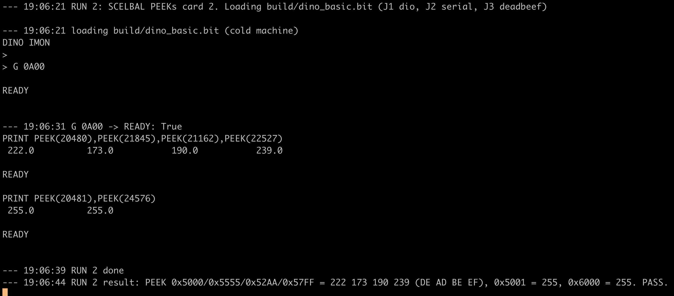
The mainboard’s eight slot sockets, J1 to J8, are eight copies of one card interface. A card drawn in KiCad and a card written by hand in Verilog plug in the same way. The first hand-written one is a card that answers DE AD BE EF, and SCELBAL reads it with PEEK.
So there are three DINOs now: the breadboard, netsim (the same netlist simulated with gate delays in Icarus) and this one. The FPGA twin proves the logic of the drawing, not its timing. Gates are zero-delay and everything moves on a 48 MHz system clock, so the analog stuff that bit the breadboard can’t show up here.
Why bother while the boards are at fab
Rev 1.0 is at PCBWay. I want to work on the next cards (CF, maybe a floppy hack) before there’s copper to plug them into, and anything I prove in RTL has to have a known route to a real card. That means the twin’s slots have to look like the real backplane, pin for pin.
The first build ran at 93.75 kHz and I thought DINO was slow
The first version of the twin divided 12 MHz down to a 93.75 kHz CPU clock, about 11 times slower than the breadboard’s 1.024 MHz. I didn’t catch that it was a slowdown and read the sluggishness as DINO’s. A SCELBAL line with a float PRINT took 2.5 minutes. Serial stress tests failed all over the place: any line over 15 characters typed back to back lost everything past the 16-byte receive ring.
Moving the system clock to 48 MHz put CLK at 1.0 MHz, and most of those failures went away:
| Test | 93.75 kHz | 1.0 MHz |
|---|---|---|
| One line typed back to back, up to 73 chars | dropped past 15 | pass |
| Program pasted, 0 or 2 ms per char | drops | drops |
| Program pasted, 5 or 10 ms per char | drops | pass |
| Program pasted, 20 or 50 ms per char | not run | pass |
200 lines of PRINT I,I*I | test timed out | pass, 5129 bytes |
| Typing while it prints | test timed out | pass |
Ctrl-C out of GOTO 10, warm start, LIST | pass | pass |
Pasting at 0 to 2 ms per character still drops input, because the 16-byte ring has no flow control. Expect the same on the real machine. A terminal set to 5 ms per character pastes cleanly.
With input echo-paced, SCELBAL on the Versa is byte-identical to the original 1974 SCELBAL running on an 8008 emulator: 11 sessions, 2409 bytes. PROG_isa reads 0xB4.
One card interface for all eight slots
Every card, generated or hand-written, has exactly the same ports. For each of the 37 edge pins that isn’t a power rail, named by pin number and signal (e8_W0, e39_M11), there’s what the rest of the machine drives on the pin and whether anything does, plus what the card drives and whether it does. There’s no inout anywhere, so the whole thing synthesizes, and any time two things drive the same net the twin raises a contention flag.
| Slot | Card | Kind | Window |
|---|---|---|---|
| J1 | card zero, DIP switch | KiCad | 0x4000 |
| J2 | serial card, 16550 | KiCad | 0x4800 |
| J3 | DEADBEEF | hand-written Verilog | 0x5000 |
| J4-J8 | empty |
A slot is a position, not an address. Each card decodes its own 2K window with a ‘138 on M11-M13, the same way the drawn cards do, so the same card works from J3 or J8. Adding a card is a Verilog file copied from the prototype card, an entry with its oracle model, and one line in the slot table.
DEADBEEF in J3
The DEADBEEF card returns DE AD BE EF at 0x5000, 0x5555, 0x52AA and 0x57FF and 0xFF everywhere else in its window. Between those four addresses every one of M0-M10 toggles, so a stuck or swapped address line reads a wrong byte. A ROM image reads the four cells, two 0xFF cells and one address in an empty slot’s window, and shows 0x5A on OB if all seven match. On the Versa the LEDs showed 0x5A.
The serial card got its edge connector
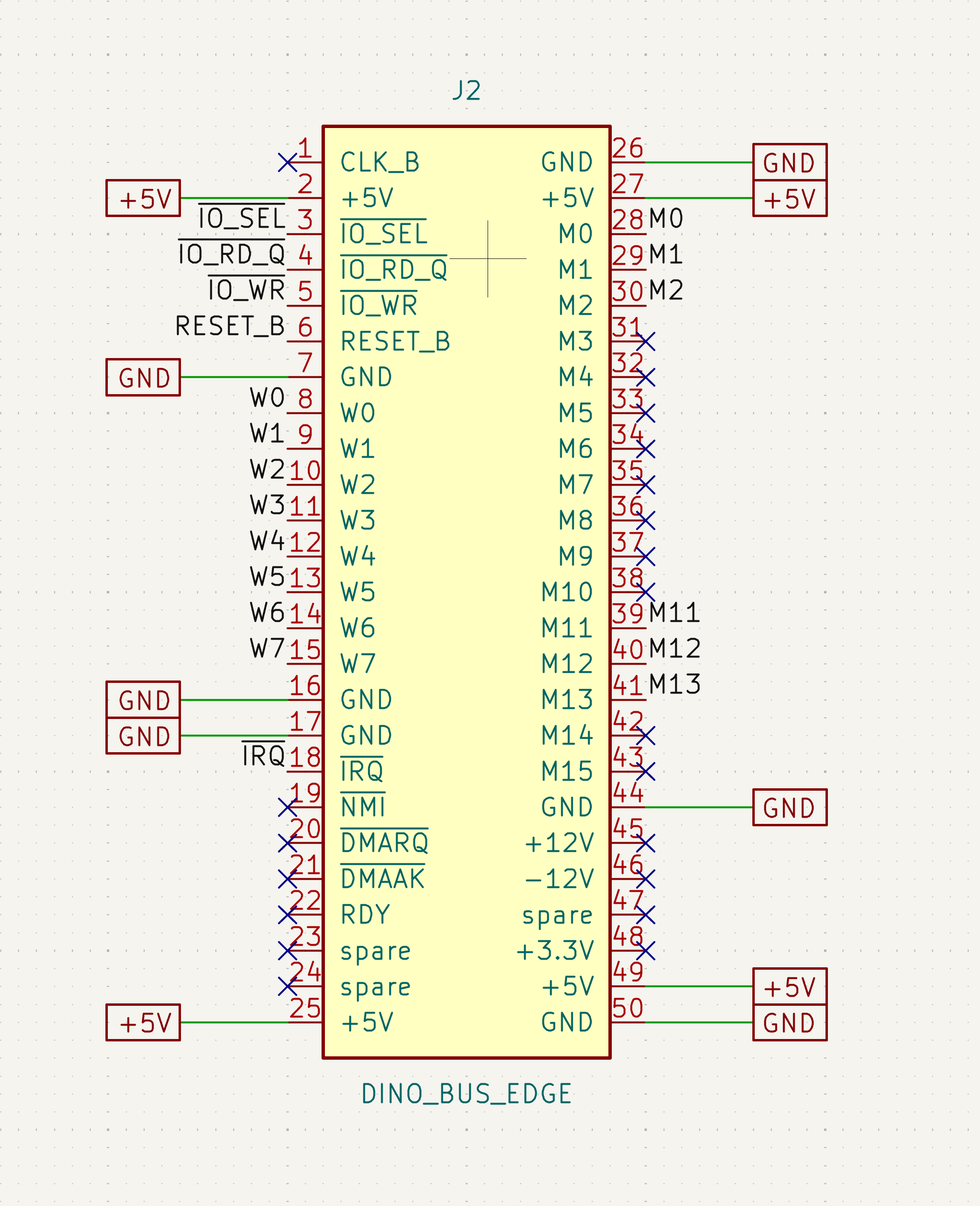
The serial card’s schematic never had an edge connector. Its bus signals were just labels. I added J2, a DINO_BUS_EDGE, with each label the sheet already had sitting on its pin. The netlist didn’t change apart from J2, and ERC went from 34 items to 3; the 3 left were there before.
Mandelbrot on the Versa
The Mandelbrot RAM program from 10-06 loads with L and runs with G 8100, same as on the breadboard, and the picture is byte-identical to the reference model.
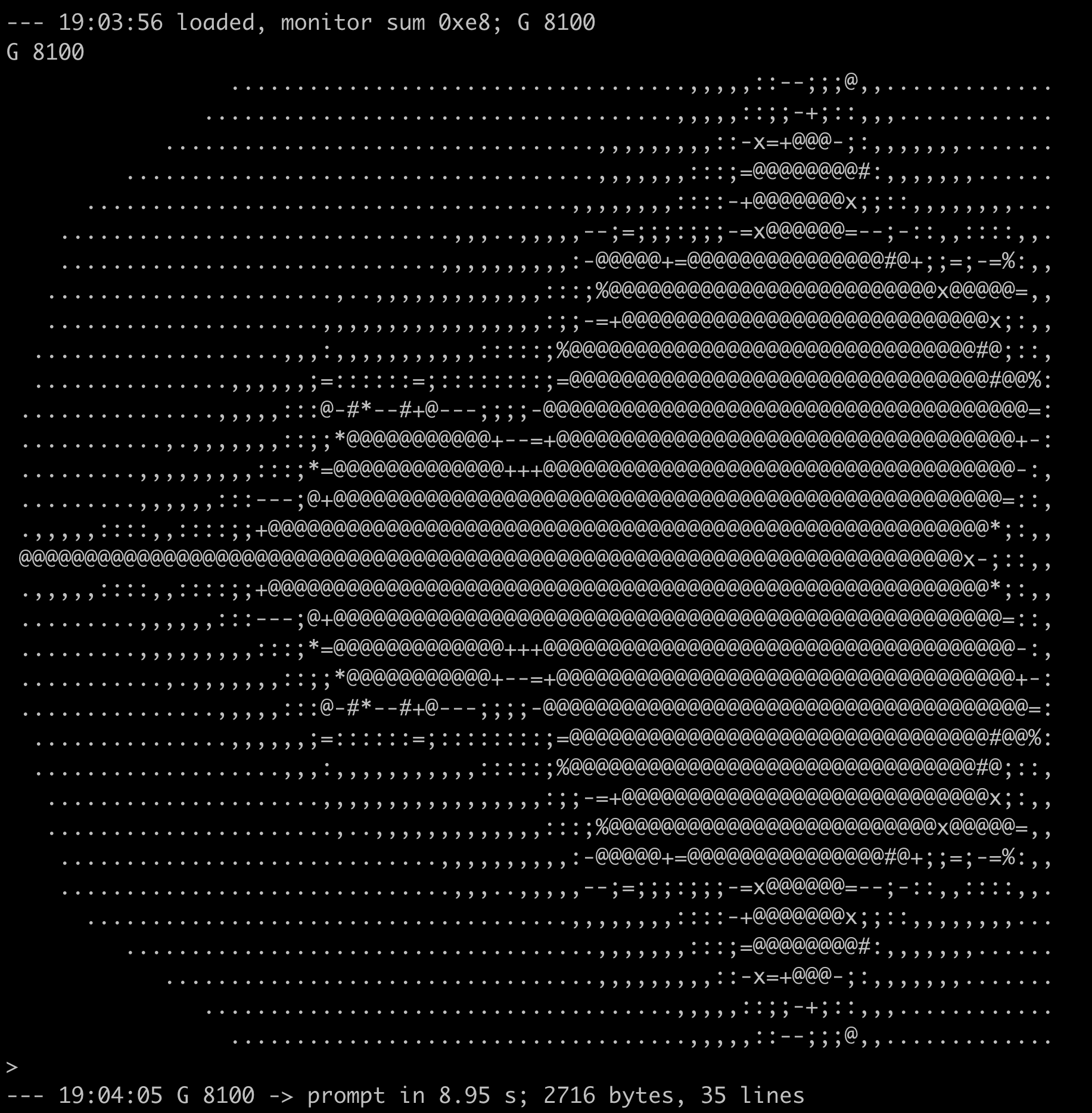
It took 8.95 s from G to the prompt, which matches the 8,717,660 T-states the oracle counts for the run.
What checks it
| Check | Result |
|---|---|
| Every coverage image, 3 power-up seeds, against the oracle | 132/132, no contention |
| Chip pins against all three netlists, every part model against netsim’s | 32/32 |
| Slots, cards, card interface, oracle with the slot table | 37/37 |
| Deliberately planted faults (pin swaps, a crossed edge pin, a miswired slot, part model bugs) | 17/17 caught |
| Whole host test suite | 725 passed |
| Versa bitstream timing | 123.6 MHz Fmax against a 48 MHz clock |
Rebuilding the twin around the slots left every result from before it byte-identical, down to the tick counts.
The breadboard runs these programs, and netsim and the FPGA twin run them from the Rev 1.0 netlist and agree, so I feel good enough about Rev 1.0 to order the boards.
Open threads
- The serial card still needs a physical edge card before Rev 1.0 can run the monitor.
- netsim has no card slots. Only the FPGA twin can seat a card for now.
- Next card in RTL: the CF card.