16-bit control word, four decoder banks, sixteen T-states
Backfilled from a post on embedded.greygiant.com dated 2025-07-25. The notebook block diagram is dated 2025-07-20.
What I tried
A week of reading and notebook work before any wire. Malvino for the SAP timing, Ben Eater’s 8-bit build for how a ROM-based control matrix and bus enables look in practice, Harris and Harris for the microarchitecture chapters, Patterson and Hennessy for datapath and control together. Then: write down the instructions, write down every data movement they need, enumerate every enable, group the enables so one ‘138 can decode each group, and sequence it across T-states.
The control word
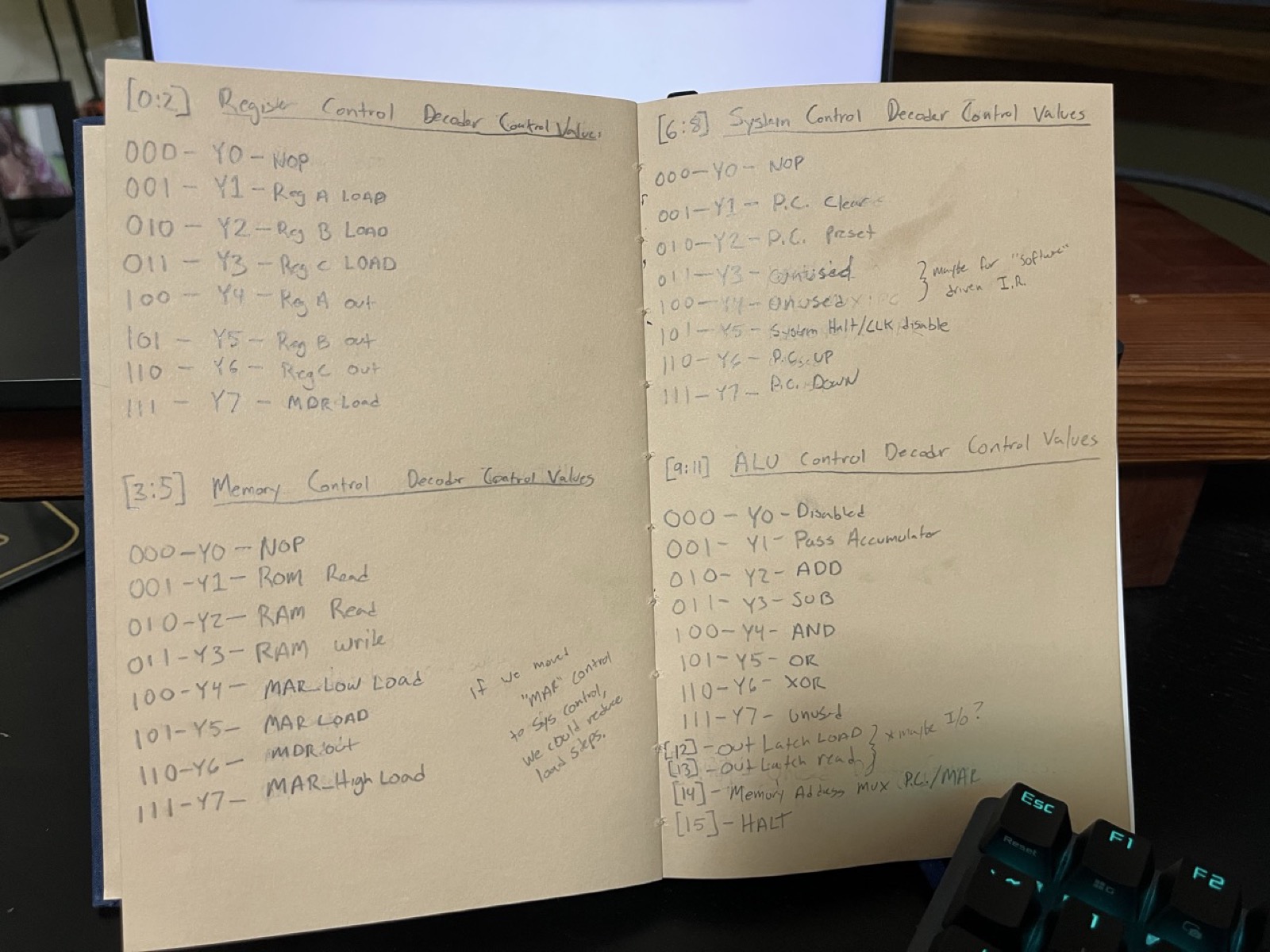
16 bits. Four direct bits at the top and four 3-bit fields, each feeding a ‘138 so at most one output in a bank is active at a time:
[15]    HALT
[14]    address mux, 1 = PC, 0 = MAR
[13]    output latch read enable
[12]    output latch load enable
[11:9]  bank 4, ALU: off, pass A, ADD, SUB, AND, OR, XOR
[8:6]   bank 3, PC: clear, preset, halt/clock stop, increment, decrement
[5:3]   bank 2, memory: ROM read, RAM read, RAM write, MAR lo/hi/full load
[2:0]   bank 1, registers: A/B/C load, A/B/C out, MDR load
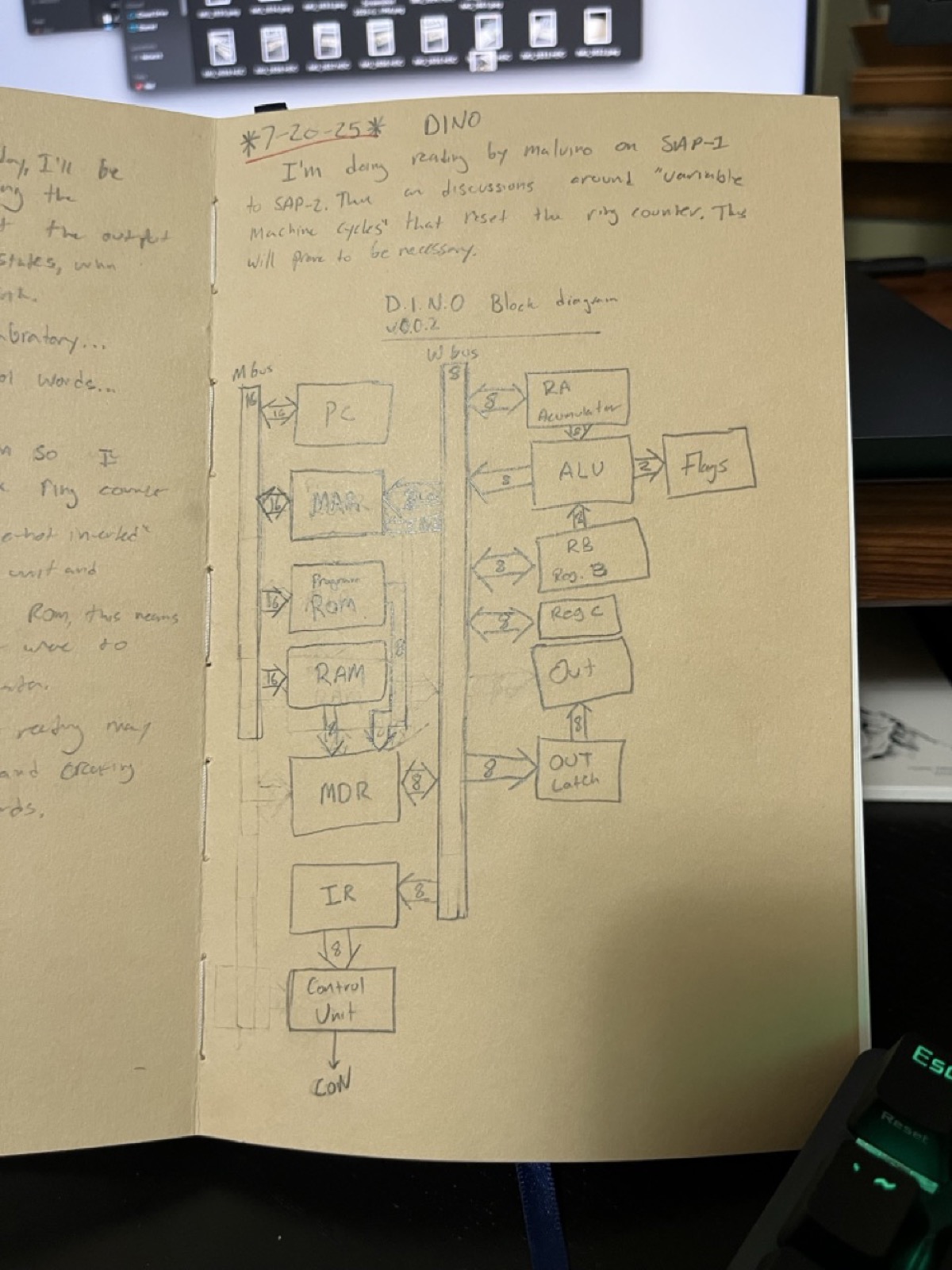
Grouping into banks is what keeps the bus from having two drivers on it. Everything in bank 1 that puts a register on the bus is mutually exclusive by construction. The banks have been reshuffled more than once since, but the control word is still decoded this way.
Sixteen states
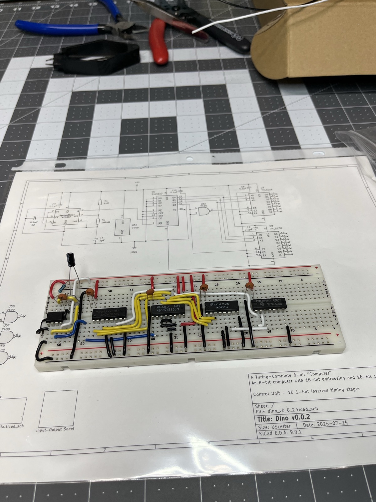
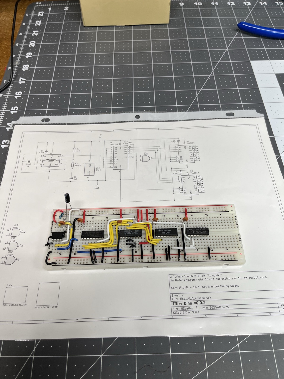
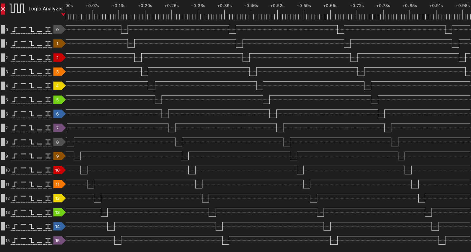
Writing out STA showed the problem with six states. Fetch is T0-T2, then it needs two ROM reads for the address bytes, two transfers into the MAR halves, and the write. Eight states. So the ring went to sixteen: the ‘163 counts 0 to 15 and rolls over on its own, so the reset NAND is gone. Two ‘138s split the range, QD through a ‘00 inverter enables the first for T0-T7, QD straight in enables the second for T8-T15.
The first four instructions
LDAI 0x11   T3 ROM read, mux=PC, MDR load, PC++   T4 MDR to A
LDBI 0x12   same, T4 MDR to B
STA  0x21   T3/T4 address lo to B, hi to C, PC++ each
            T5 B to MAR lo   T6 C to MAR hi   T7 A to RAM
STB  0x22   as STA with A and B swapped for the address parking
T0-T2 are the same for all of them: opcode to MAR and IR, PC into MAR, branch on the opcode. STA parks its address bytes in B and C on the way to the MAR because the MAR loads in halves and there’s nowhere else to put them.
The test program
LDAI 0x0D
LDBI 0x02
STA  0x0001
STB  0x0002
NOP
LDA  0x0002
LDB  0x0001
ADD
MOVAC
OUT C
HLT
Immediate loads, 16-bit address formation, store, load back, add, register move, output, halt. It’s the program the whole datapath has to run before I’ll believe any of it.
What I measured
The 16-state ring on the LA, clean, at 60 Hz off the 555. Nothing else exists yet to measure.
Next
Burn the control word ROM. Build the IR and connect it to the ring. Then the datapath.