DINO
D.I.N.O., Discrete Integrated NISC Operator, is an 8-bit CPU I built from 77 discrete 74-series chips on breadboards, designed in KiCad. Three AT28C64B EEPROMs hold a 24-bit microcode word; program ROM is an AT28C256, RAM a 32K MCM60256. It started as a 25-instruction machine that could add two numbers and has grown, phase by phase, into a 174-instruction ISA with a 16-bit stack pointer, CALL/RET, execute-from-RAM, a 16K memory-mapped I/O window with eight card slots, a 16550 serial card, and a ROM monitor that loads hex over the wire and runs it. Most of the hard faults turned out to be analog stuff, not logic. The breadboard is at the end of what it can do at 1.024 MHz and the next phase is a PCB, power first.
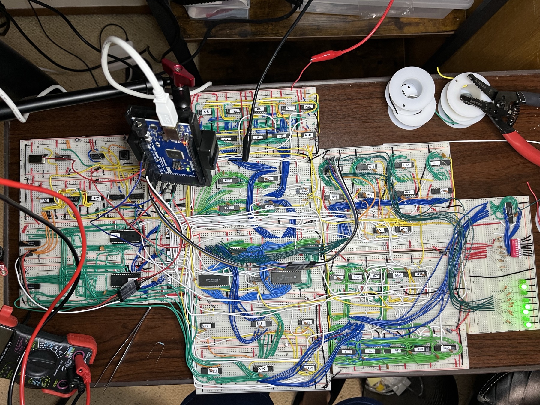
Current state
As of 2026-09-10: The machine is complete and runs the whole ISA from ROM at 1.024 MHz. PROG_isa reads 0xB4 (147 subtests pass) and PROG_isasoak read 0x00 on 50 consecutive runs, 470,400 subtest executions, zero miscompares, after GND and VCC were starred to every board on 2026-09-01.
Phases B through G are on silicon: stack (B), CALL/RET (C), execute-from-RAM (D), the 16K I/O window at 0x4000-0x7FFF with the DIP switch as card zero (E), the 174-instruction ISA (F), the 16550 serial card at 9600 8N1 (G), and the ROM monitor with D/W/O/L/G commands (G_0). All 32K of RAM, 0x8000-0xFFFF, is proven for data and for fetch.
RAM-resident programs run. The monitor’s L command loads hex over serial with dinoload.py pacing one character per echo, and G runs it. The 2233-byte bigxfer transfer has gone in and streamed itself back clean several times, sometimes back to back; what stops it is mechanical, a table bump or a wire out of line, and I think every error on this breadboard has been noise. The one pinned timing fault is OUT immediately before a fetch from RAM: it halts at 1.024 MHz and returns at 500 kHz. A microcode settle row was burned and did not fix it. It’s setup margin lost to breadboard bus capacitance.
Decision 2026-09-08: the breadboard phase is over. Next is one 2-layer mainboard with the phase E slots as its only connectors, and power gets designed first. The machine draws 1.25 A to 1.34 A at 5 V on the bench supply ammeter. The supply itself is an open item, old ATX unit or PicoPSU, not dug into yet.
Architecture
Horizontal microcode, no instruction pipeline. Each opcode is a table of rows in a 24-bit control word held in three AT28C64B EEPROMs (U9, U15, U23); T0 is the universal fetch and a 74LS163 T-counter steps the rows until END. Every state-changing load is clock-qualified and commits on CLK low; bus output enables are ungated. The machine is fully static, so the clock can stop.
Two buses. MDR0-7 is the internal bus (ROM, RAM, registers A/B/C, stack pointer halves, PC halves all drive it through ‘245s). W is the ALU and destination side. A ‘245 bridge (U25) joins them whenever any source is active, so a destination can latch from either side: MAR and IR latch from W, registers from MDR. The ALU is a pair of 74F382s with ripple carry; all four flags latch in a ‘273 and update only when the ALU is the source.
Memory map: ROM at 0x0000-0x3FFF, the I/O window at 0x4000-0x7FFF decoded into eight 2K card slots on M11-M13, RAM at 0x8000-0xFFFF. Card zero is the DIP switch at 0x4000. Card one is the serial card at 0x4800. Cards see the address bus as an input only; there is no DMA by construction.
ISA: 174 instructions. Immediate and register ALU ops, absolute and memory-indirect loads and stores (LDAM/STAM parks a pointer through C and MDR), conditional branches on C and Z, PUSH/POP, CALL/RET, OUT to an 8-LED latch that latches MDR. CALL pushes PC+1 and RET steps over the two operand bytes with trailing PC_UP states. The high nibble of an opcode is its family so a byte is hand-disassemblable at the bench.
Tooling is all generated from the KiCad schematics: the netlist oracle extracts gate equations, kicad_contracts.py emits landing and change lists for the copper, microcode_gen.py emits the ROM images with pinned CRCs, and a Python oracle in progrom_gen.py interprets the real microcode rows to compute what OB should read for every coverage image.
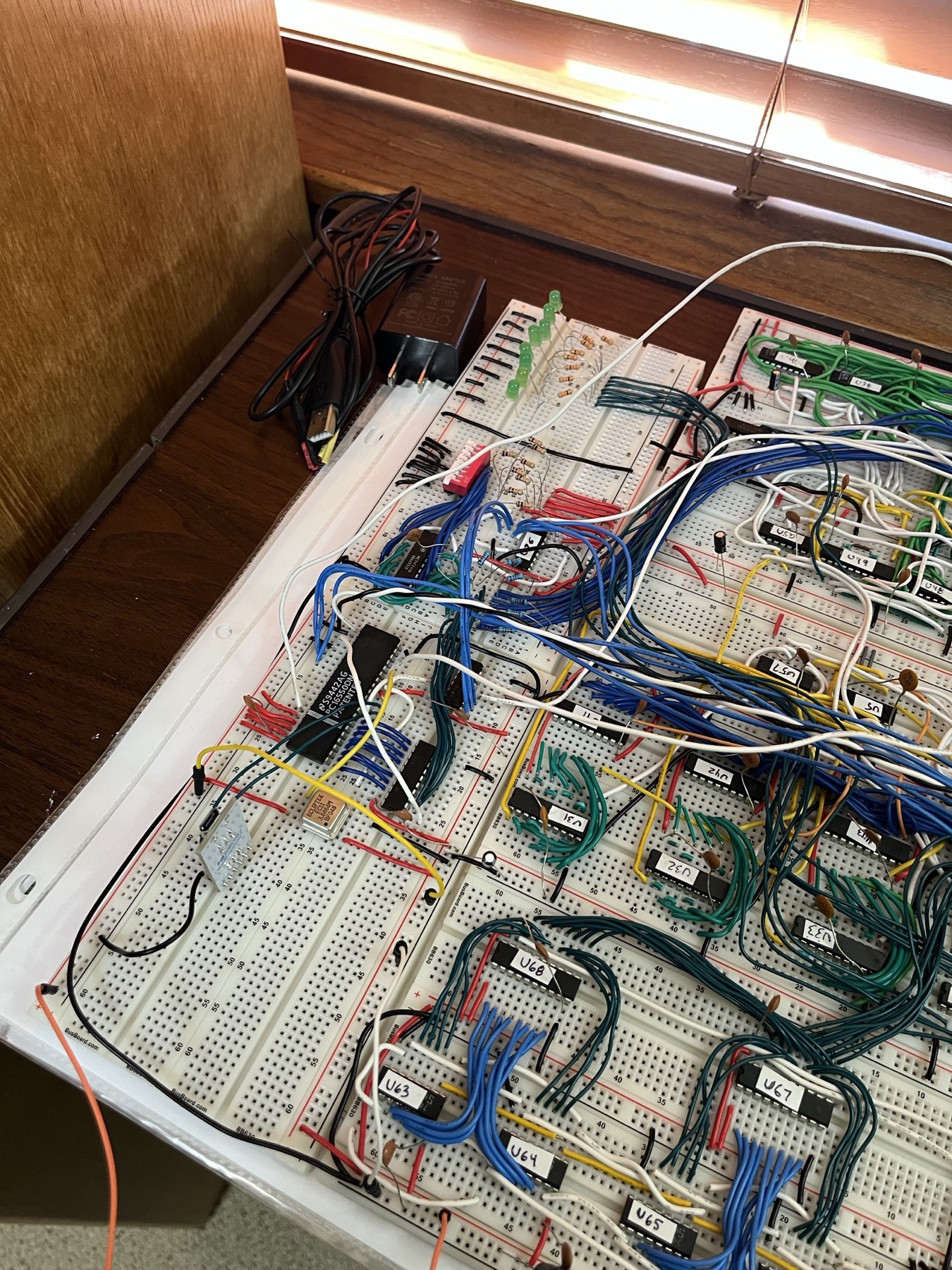
The DIP switch and the serial card are both just memory. Adding a peripheral is a ‘138 decoding its 2K slot on M11-M13 plus whatever chip does the work; the core doesn’t change. That part’s easy now. The breadboard is what’s in the way.
Hardware
77 ICs on the core, ten breadboards, plus a 3-IC serial card. Netlist count 2026-09-08:
17  74LS245      11  74LS373     9  74LS138
 8  74LS02        4  74LS169     4  74LS193      3  74LS08
 3  AT28C64B      2  74LS163     2  7400         2  74LS157
 2  74F382N       2  74LS244N    2  74LS00       1  74LS74
 1  74LS14        1  74LS273     1  74LS32       1  74LS04
 1  MCM60256AP    1  AT28C256    1  PC16550D
 8  LED (330R)    2  oscillators (4 MHz can, 3.6864 MHz can)
Single +5 V rail. The core clock is the 4 MHz can divided down to 1.024 MHz; a 500 kHz option exists for timing discrimination. The serial card runs the 16550 off the 3.6864 MHz can and an FTDI TTL cable.
Analog fixes that are now part of the design: a 100R series resistor (R2) in the stack pointer board’s CLK branch, without which the ‘169s double-clock; a 10uF reset capacitor (C1) after a 1uF was found in the socket and gave a 0.8 ms runt instead of a power-on reset; GND and VCC starred to every board after the ground pins measured 142 mV to 460 mV above the supply terminal; and the RESET wire pulled out of the bundle with CLK and the buses, where it picked up 1.5 V runts.
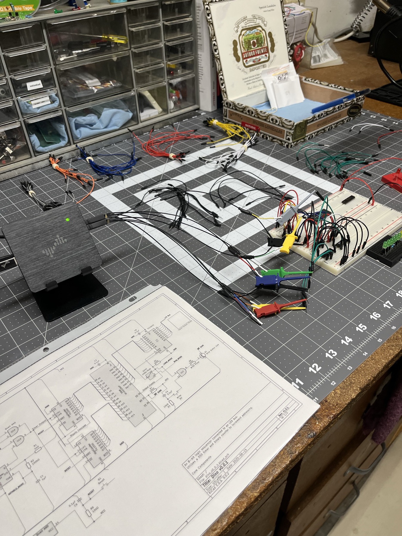
Instruments: DSLogic LA (20 MHz max), Siglent SDS1204X-E, DMM, TL866 programmer. The ATmega2560 test rig and the FPGA twin are both retired.
Gateware and firmware
Decisions
2026-07-28: integration is control-first and black-box. Blocks are tested by sampling only signals whose value depends on more than one member; driven-wire count is the gate and may not rise.
2026-08-24: the ATmega2560 rig is retired. Bench verification is continuity against the generated crossing list, TL866 read-back, and the coverage ROMs’ OB values.
2026-08-24: the FPGA twin is retired, not repaired. It generates from the schematic, so it cannot see a build error or an analog fault, and every fault that killed it was one of those.
2026-08-25: phase E (memory map plus DIP card), F (ISA extension) and G (serial card) are independent of each other in both directions.
2026-08-27: 0x00 stays NOP. A NOP slide is a legitimate idiom; HALT at 0x00 would make a mistyped immediate stop the machine.
2026-08-27: IN is retired from the ISA. SW1 is memory at card zero.
2026-09-01: computers are analog. When a fault is not in the program, measure the rails before building a logic model.
2026-09-04: ROM readable as data is fixed in copper (three re-sourced pins), not worked around in software.
2026-09-07: RAM 0x8000-0xFFFF is proven whole. If a RAM program freezes, it’s the control path, not the RAM.
2026-09-08: the breadboard phase is over. One 2-layer mainboard, the phase E slots as its only connectors, and power is designed and measured first. S-100 style cards rejected.
Never commit or push without an explicit ask. Never write an assertion from a reading of the schematic; extract the gate equation from the netlist first.
Grounding rules for the PCB, earned 2026-09-01 and 2026-09-05: ground is a wire with voltage across it; ground plane; supply entry at the centre, star or per-board power entry; every external ground (USB, scope clip) enters at the star only. Check: supply current with the FTDI unplugged must equal supply current with it plugged. The serial card’s row had been grounded to the FTDI, not the machine, and 250 mA of return current was leaving through the laptop.
Route RESET away from CLK and the buses. It picked up 1.5 V runts in the breadboard bundle and reset the UART’s LCR and FCR at random.
Every board that puts raw CLK on a clock pin at the end of a stub gets series termination. R2 100R on the stack pointer board is the precedent.
2025-07-18: control words come out of an EEPROM addressed by opcode and T-state, not out of gates the way Malvino draws it. Still how the machine works, three EEPROMs later.
2025-07-25: the control word is decoded in 3-bit ‘138 banks so the sources on a bus are mutually exclusive by construction. The banks have been reshuffled since; the scheme hasn’t.
Open problems
- OUT immediately before a fetch from RAM halts at 1.024 MHz and returns at 500 kHz. Setup margin of 488 ns to 1000 ns is not in the datasheet path (382 ns worst case to IR); it is breadboard bus capacitance plus the REG_A to RAM buffer cross-driver handoff. Workaround for now: don’t put OUT right before RET in RAM code. The PCB should fix it properly.
- Breadboard mechanical noise. bigxfer transfers clean several runs in a row, then a table bump or a wire out of line stops it. Not a logic fault and not worth chasing on breadboard.
- Power supply for the PCB. Draw is 1.25 A to 1.34 A at 5 V, single rail. Candidates: the old ATX unit on hand (free, PWR_OK is a real power-good the machine has never had, but an old unit is likely group-regulated and may need a dummy load on 12 V), a PicoPSU (independent rails, two conversions to reach one 5 V rail), or a plain regulated 5 V brick (one conversion, no power-good, so a supervisor IC on the board). Not dug into yet. POWER.md has the comparison and the bench tasks: ATX rail in spec and under 50 mV ripple at DINO’s load, and whether it is group-regulated.
- Whether run, idle and halt draw differ. LS245 Icc is highest tri-stated, so a quiet bus can still run warm. Decides decoupling.
- The OUT settle row burned into U15 (CRC 0x45F9) fixes nothing and costs a T-state. Revert on the next burn, together with the 23 SETTLE rows added for a fault that turned out to be ground.
- CN+4 after a logic function on the 74F382 has never been measured; the oracle refuses to answer a JNC that depends on it.
- 22 instructions and the 15-opcode OUT_ family have never executed on silicon. Microcode-soft, not hardware.
- U9 sits in a marginal socket after the chip swaps of 2026-09-05; a post-HALT ~WR strobe traces to it. Socket replacement pending.
- Bus levels have never been characterised on a healthy machine.
Links
- Repo: https://github.com/robertrico/dino-homebrew
- Schematics:
dino_v0_0_2/anddino_serial/in the repo (KiCad) - Coverage ROM table with expected OB per image:
roms/README.md - ISA roadmap:
docs/notes/dino_isa_for_basic.md