Rev 3 is laid out, and the transceivers had to go down first
Rev 3 is laid out. I’m laying out a new board because Rev 2 can’t be updated with its own parts. Its 74LVC8T245 level shifters and its FTDI USB chip are both out of stock. Rev 3 is an LFE5U-25F in TQFP-144, four 8 MB QSPI PSRAMs, 74LVC245 transceivers with DMA wired up, open-drain drivers on the shared slot lines, and no USB. The board is 114.5 x 69.55 mm on 4 layers and KiCad’s DRC is clean: 0 errors, 0 unconnected, schematic parity clean. The BOM is priced from live DigiKey and Mouser data through two CLIs I wrote for it. Parts come to $47.10 a board for five at DigiKey, all in stock. On 2026-11-06 I checked the layout against the datasheets, found eight things to change, and put them on the board in a fourth pass the same day. The main one was sixteen pull-up resistors that are too weak for an ECP5. All of it is further down.
It took two days and three layout passes to get a clean board, and a fourth to carry what the datasheet check found. The first pass routed and passed DRC and was still bad, with slot nets averaging 82.7 mm against 16.5 mm on Rev 2. What fixed it was placing the parts the way I placed Rev 2 by hand: transceivers first, sitting on their fingers, then the FPGA, then everything else.
Rev 2 is frozen and Rev 3 started from the parts list
Rev 2 is tagged rev2 in git. Rev 3 is a copy of the KiCad project in hardware/byte_hamr/kicad_rev3/, sitting next to Rev 2’s so the two layouts can be compared side by side. I started with the BOM and priced it before drawing anything, using a DigiKey CLI I wrote (dkp) and a Mouser one beside it. Low cost is the first rule for Rev 3.
| Part | Choice | Why |
|---|---|---|
| FPGA | LFE5U-25F-7TG144C | TQFP so everything goes on the top side. -7 is the only speed grade DigiKey stocks (103 pcs, $22.33); -6 and -8 have an MOQ of 300. Any grade is fast enough for a IIe. |
| RAM | 4x ESP-PSRAM64H, 8 MB each | $1.75 each at DigiKey. AP Memory’s APS6404L isn’t sold there; Mouser has it at $2.90 as the fallback. |
| Config flash | GD25Q128ESIGR | $2.98 against $5.99 for the W25Q128. Disk images still live in flash, so it stays 128 Mbit. |
| Bus logic | 6x 74LVC245A, 74LVC125A, 74LVC07A | Commodity SOIC parts at 3.3 V with 5 V tolerant inputs. Rev 2’s 74LVC8T245 is out of stock. |
| Power | Rev 2’s three TLV62569 bucks | Unchanged. |
| Passives | 1206 everywhere | Easier to rework. |
DigiKey has all 26 lines, Mouser is missing five
The BOM is a CSV with one row per job and 26 part numbers once same-value rows are merged. dkp bom and mouser bom each price the whole thing in one go. These are the 2026-11-06 runs, after the fourth pass added five resistors and split the header fuses into two parts.
| DigiKey | Mouser | |
|---|---|---|
| 1 board | $52.62 | |
| 5 boards | $235.48, $47.10 a board | $241.87 for what it can supply |
| Coverage | All 26 lines in stock | 3 lines not carried (the Jauch oscillator and both Sullins headers), 2 at 0 stock (74LVC07A and the Murata inductor), FPGA -7 at 0 with an MOQ of 300 |
That’s parts only. It leaves out the PCB, a stencil, and the external Pico 2s. Before the fourth pass it was $51.34 for one and $46.06 a board for five; the 1.1k pull-ups cost more than the 10k ones.
| Share of the 1-board cost | |
|---|---|
| FPGA | $22.33 (42%) |
| 4x PSRAM | $7.00 |
| 6x 74LVC245A | $3.36 |
| Flash | $2.98 |
| Everything else | $16.95 |
Mouser’s figure uses its -6 speed grade of the FPGA ($24.05, 190 in stock) and the APS6404L PSRAM ($2.71 at 20) in place of the two parts it doesn’t sell. It is still worth having beside DigiKey for exactly those two.
Every FTDI USB chip is out of stock, so USB came off the card
The FT231X on Rev 2 does one job: it bit-bangs JTAG through its modem-control pins. The FT231XQ, FT231XS, FT230X, FT232R, FT232H and FT2232H all showed 0 stock at both DigiKey and Mouser, with Mouser quoting 210 to 294 days. I looked at putting an RP2354A on the card instead and dropped it, because it would have grown into its own subsystem with its own firmware. Rev 3 keeps only Rev 2’s 2x3 JTAG header. Each card gets its own external Pico 2 running pico-dirtyJtag on a short ribbon, with a long USB cable out of the case. openFPGALoader already supports dirtyJtag. The JTAG lines on the card have 1.1k series resistors, so a powered Pico can’t push much current into an unpowered FPGA.
Two layers never routed
I tried 2 layers first because they’re cheaper. On Rev 2’s 97.6 x 67 mm outline Freerouting was still 36 to 81 connections short after each pass. At 160 mm wide, 13 runs plateaued at 6 to 20 unrouted. The board went to 4 layers: F.Cu and B.Cu for signals, In1 as a solid ground plane, In2 for power.
Pass 1 routed and passed DRC, and the layout was still wrong
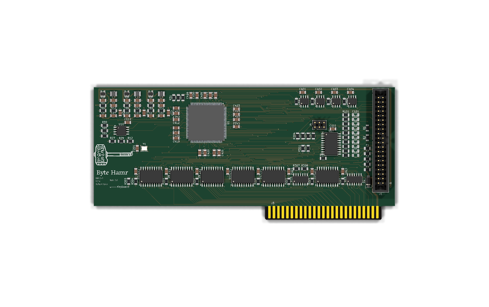
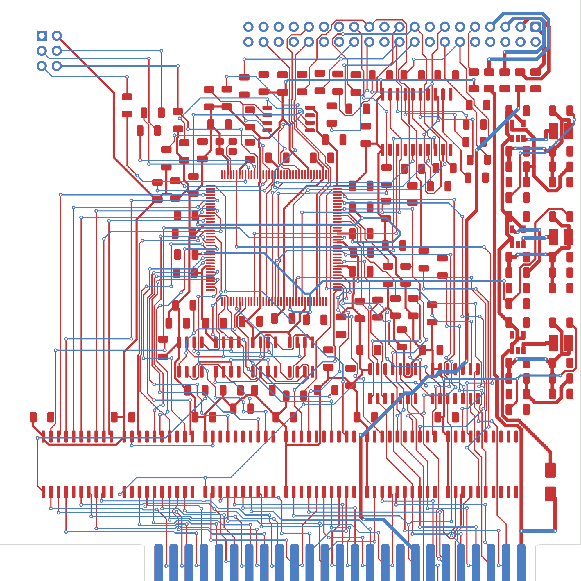
Pass 1 was placed by optimizing total wire length with an annealing placer, then loosened up for spacing. The FPGA pin map had been designed before any of that, by package side: address and data on one side, slot control on the opposite side. That was the wrong assumption. I expected the router to untangle any pin order, and with a TQFP every crossing between the pin order and the transceiver order costs a via. Pass 1 needed 677 vias and 11.9 m of track. The slot nets, which should be the shortest wires on the board, averaged 82.7 mm.
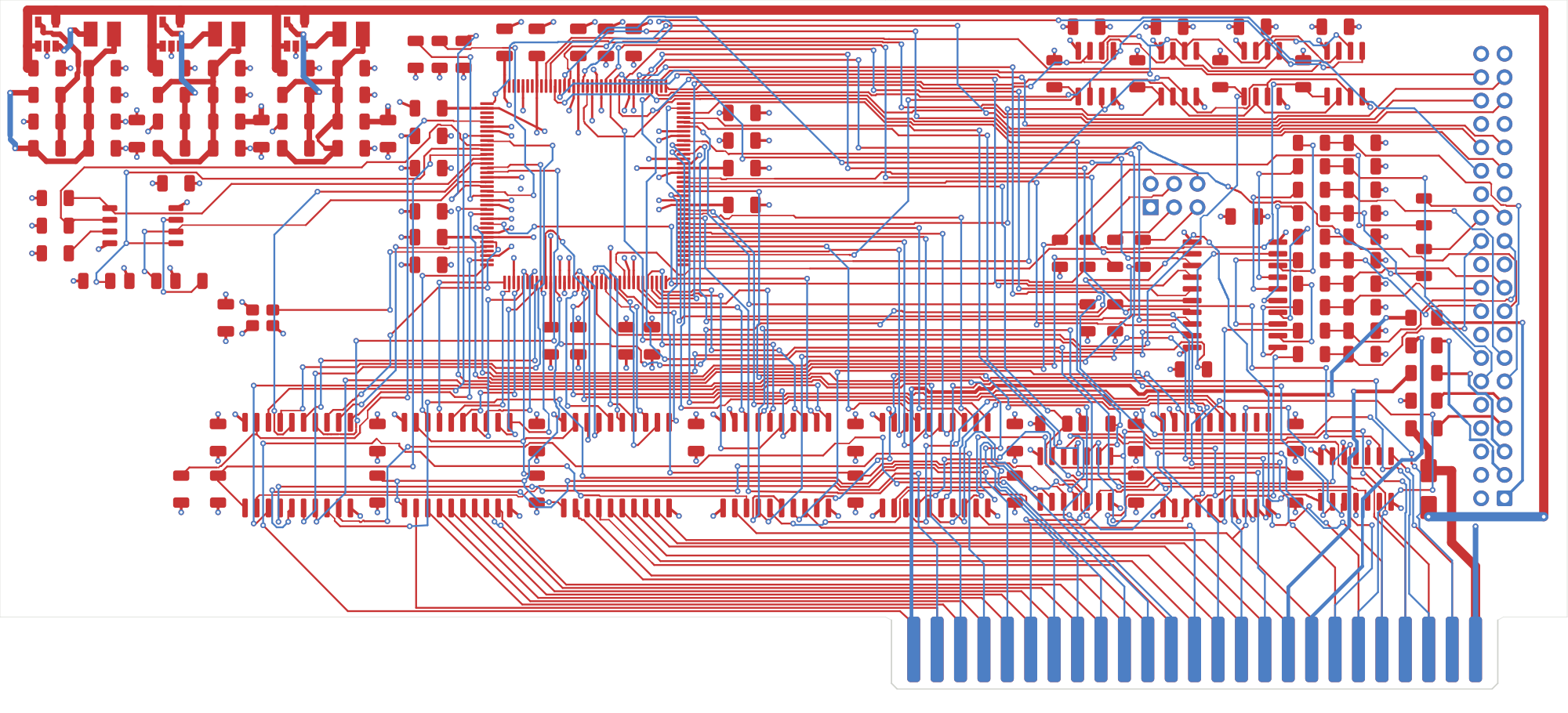
Placing it the way I placed Rev 2 by hand
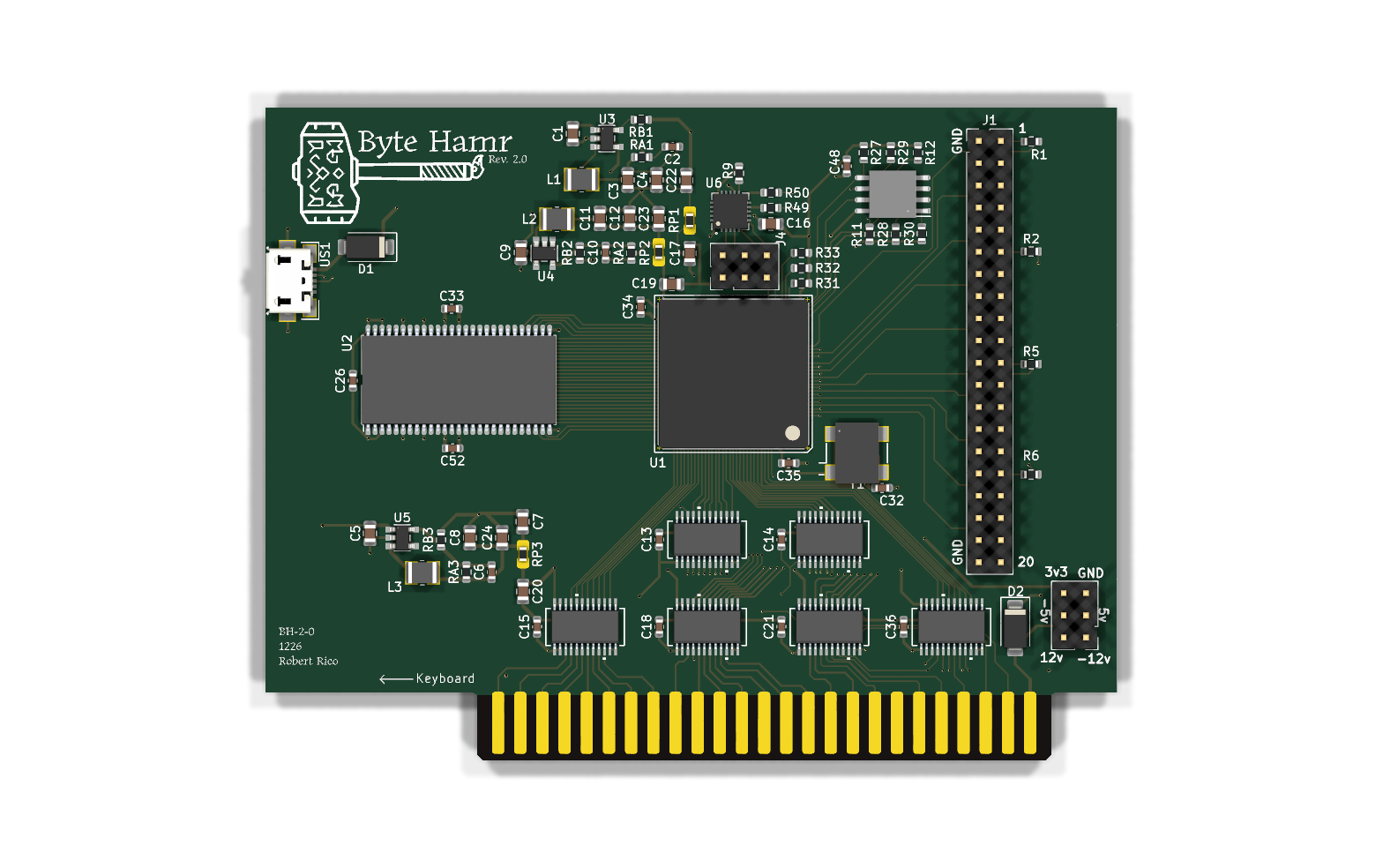
On Rev 2 I put the transceivers down first, close to the fingers, in two staggered rows: a lower row at a 14 mm pitch and an upper row offset into the gaps. The fingers get assigned to chips left to right across both rows, so a lower chip and the upper chip next to it share the first block of fingers, and the upper chip’s traces run up through the gap. Then the FPGA goes as close above them as it can, and everything else lands where it fits.
Pass 2 did exactly that. The ‘245 channels were swapped to match finger order, the FPGA went straight above the rows with its bus side down, and the FPGA pins were assigned last, from the placement. The pin map comes out of the layout.
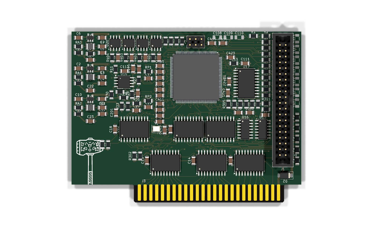
The board came out 3 mm longer than Rev 2. Slot nets dropped from 82.7 mm to 26.8 mm and total track roughly halved.
Apple’s card limits set how far it could grow
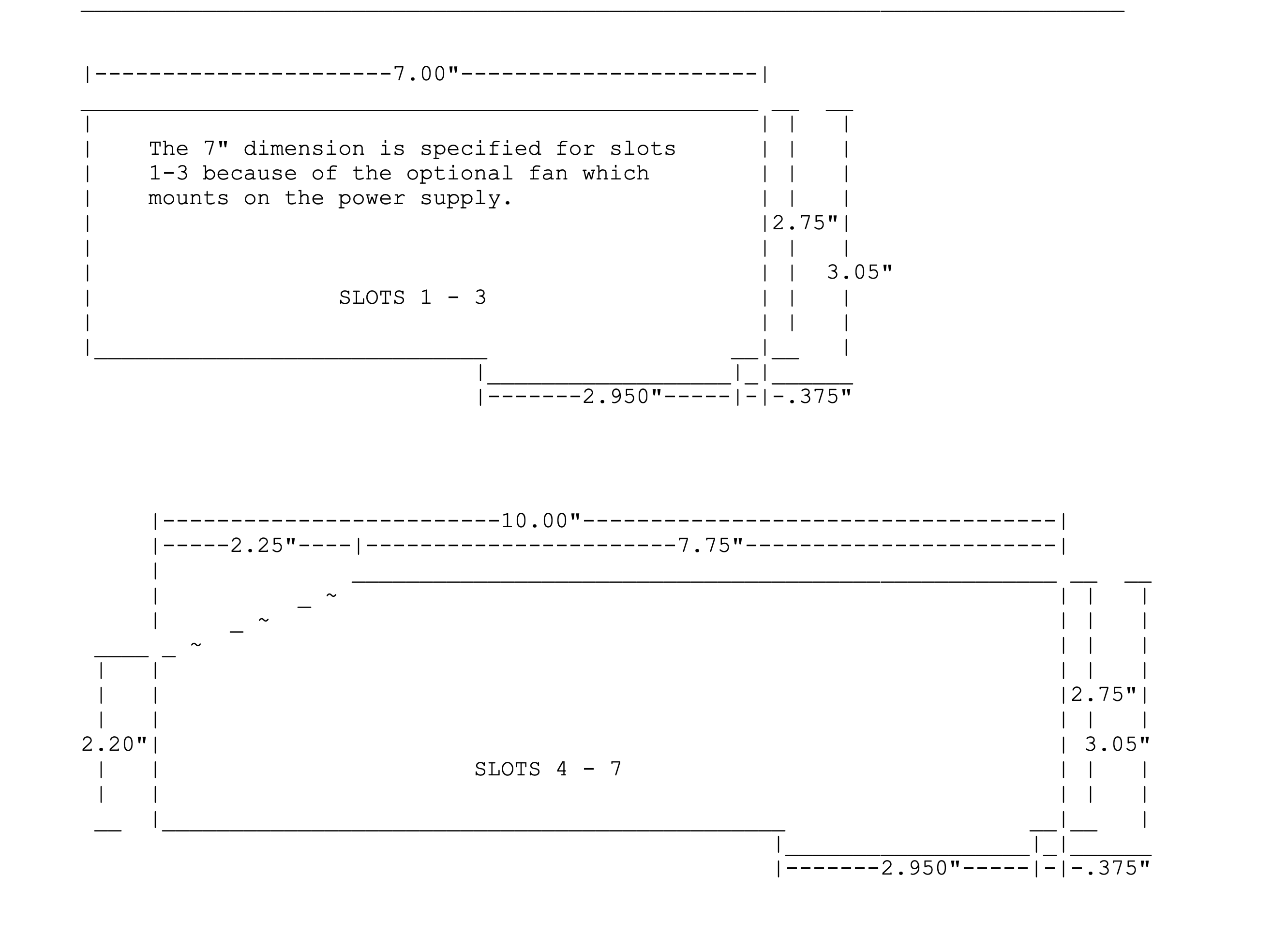
Pass 2 was dense, so I spread it. Every center-to-center distance grew 20% in x and 4% in y, with the transceiver rows and the rear edge pinned. The card only grows toward the keyboard. The rear edge, fingers and notches stay exactly as Rev 2, and the top edge went up to Apple’s limit. With Rev 2’s finger tab the card is now 77.37 mm tall, 0.1 mm under the 3.05" total. At 114.5 mm it’s far inside the 7.00" limit for slots 1 to 3. I also kept vias out of the strip 9.5 mm above the board edge; Rev 2 had 20 vias in there.
Rev 3 still covers 44% of the board with parts, against 31% on Rev 2. The 1206 passives, the TQFP’s fan-out and the pull resistors that keep the card off the bus while the FPGA loads take up most of the difference.
Freerouting’s optimizer never ran until pass 3
Passes 1 and 2 had power wiring drawn by script and kept out of the router. Freerouting doesn’t understand KiCad’s copper pours, so every pad that reaches ground or 3.3 V through a plane looked unrouted to it. Its optimizer only runs on a board with nothing unrouted, so it never ran, and every route on those passes was the router’s first complete solution. Its log says so directly:
Skipping optimization stage: the board has 1 unrouted connection(s)
For pass 3 the hand-drawn power came out. In1 is solid ground. In2 is 3.3 V with a 5 V strip cut out of it along the board edges, from the diode by the fingers up to the bucks, and a 1.1 V island under the FPGA. 2.5 V draws about 16 mA, so it’s an ordinary trace, 0.4 mm wide and 0.25 mm where it runs into the FPGA pins. Then I went through Freerouting 2.5.0’s source to see what its settings actually do.
| Setting | What it fixed |
|---|---|
--router.optimizer.enable_preflight_guards=false | Lets the optimizer run even if something is left unrouted. |
--router.job_timeout=00:30:00 | Freerouting stops itself and still writes the SES. Killing the process from outside throws the whole result away, which is how I lost one optimizer run. |
--router.automatic_neckdown=false --router.neck_width_um=150 | 2.5.0 retries a failed track at 75%, 60% and 50% of its width with no floor, which gave me 0.09 to 0.12 mm tracks. |
--router.scoring.via_costs=160 | Fewer vias. --router.via_costs is not a valid key. |
improvement_threshold 0.005 | It’s a percentage. 0.5 means 50%, and the optimizer stopped after one pass. |
| Fanout off | Fanout escapes every SMD pin with a net, 578 of 599 on this board. It adds vias. |
Native plane routing still doesn’t work on this board. Freerouting queues the plane pins and then fails every one of them, and I haven’t found out why. The plane pads get one script-placed via each instead, and the plane nets stay out of the router input. With that, routing reaches 0 unrouted in 98 to 274 seconds, and the optimizer is what takes the time, about 1 to 2 minutes a pass. I ran five variants in parallel on different via costs and kept the one with the fewest vias.
Where it landed
| Stage | Board | Vias (signal) | Signal vias per net | Track | Avg slot net |
|---|---|---|---|---|---|
| Rev 2, by hand | 97.6 x 67 mm | 242 | 4.88 m | 16.5 mm | |
| Pass 1 | 170.1 x 67 mm | 677 (469) | 2.51 | 11.88 m | 82.7 mm |
| Pass 2 | 100.6 x 67 mm | 550 (380) | 2.03 | 6.43 m | 26.8 mm |
| Pass 2, spaced out | 114.5 x 69.55 mm | 486 (306) | 1.85 | 6.54 m | 25.8 mm |
| Pass 3 | 114.5 x 69.55 mm | 402 (190) | 1.15 | 5.64 m | 24.3 mm |
| Pass 3c | 114.5 x 69.55 mm | 386 (174) | 1.05 | 5.59 m | 26.0 mm |
| Pass 3d | 114.5 x 69.55 mm | 429 (215) | 1.30 | 5.69 m | 26.7 mm |
Pass 3c is pass 3’s placement with the right-hand buffer row re-ordered to U15, U16, U14, and with the power nets routed by Freerouting ahead of the signals. Pass 3d is what the datasheet check below asked for, and it costs 43 vias: about 30 of U1’s pins now have a capacitor sitting in front of them and have to escape inward.
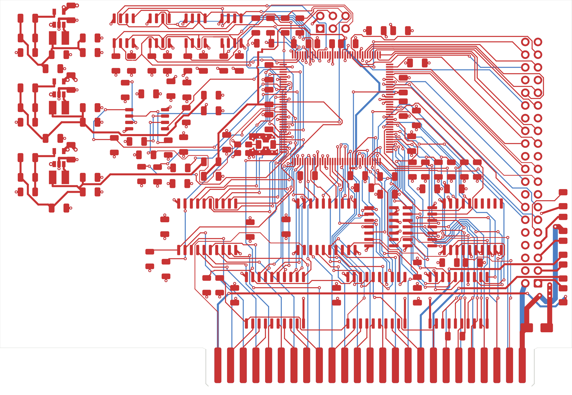
Slot nets average 10 mm longer than Rev 2’s hand-routed ones, and I haven’t dug into which nets make up the difference.
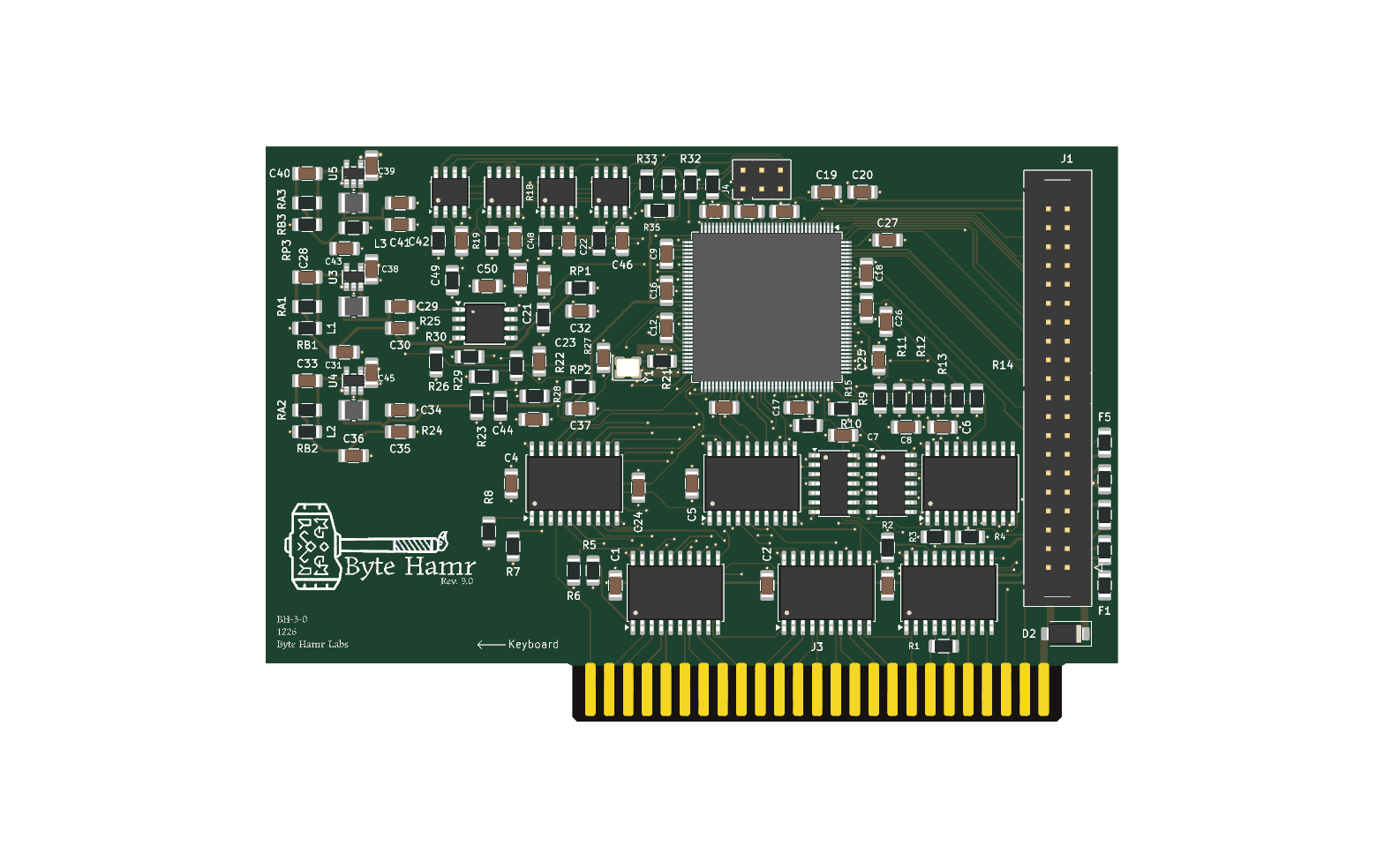
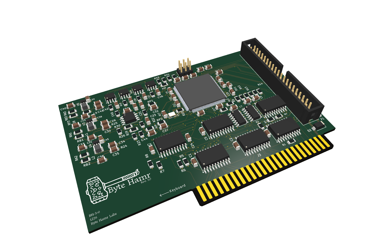
The KiCad project, BOM, pin map and spec are on the rev3 branch, one commit per pass.
Checking the layout against the datasheets turned up eight things
On 2026-11-06 I went through the layout: the exported netlist against each part’s datasheet, the board file against Rev 2’s, and Lattice’s documents for what an ECP5 pin does before the bitstream loads. DRC checks that nets connect and that copper keeps its distance. It has no rule for a resistor value or for how far a cap sits from its pin, and that’s where everything below was hiding.
| # | What | Fix | Touches |
|---|---|---|---|
| 1 | 16 bus-safe pull-ups are 10k, against an ECP5 pull-down of up to 150 uA | 1.1k | BOM only |
| 2 | FPGA decoupling caps sit 5 to 29 mm from their pins, and the 2.5 V ones are at the far end of a 63 mm trace | Caps at the pins | Layout |
| 3 | Buck input caps reach VIN only through plane vias | Caps against VIN and GND on top copper | Layout |
| 4 | INT OUT, DMA OUT, SYNC and COLOR REF inputs can float | 4 pull resistors | Schematic, layout |
| 5 | No pull-down on TCK | 4.7k | Schematic, layout |
| 6 | Header polyfuses are 0.55 to 2.3 ohms | Lower-resistance part on 5 V and 3.3 V | BOM only |
| 7 | Two FPGA pin pairs carry two always-driven clocks each | 4 pin swaps | Schematic, layout |
| 8 | openFPGALoader has an open bug on the 25F with dirtyJtag | Pick versions, keep a second cable | Tooling |
Pass 3d carries 1 through 7. Number 8 is a bench problem.
The pull-ups that hold the card off the bus lose to the ECP5’s own pull-downs
Rev 3 has 16 pull-up resistors that are there to keep the card quiet until the bitstream loads. They hold the transceiver enables off, point the direction pins at the FPGA, release the six open-drain drivers and keep the four PSRAM chip selects high. They were 10k. I assumed an unconfigured ECP5 pin floats. It doesn’t. The data sheet’s pin table says:
During configuration the user-programmable I/O are tri-stated with an internal pull-down resistor enabled.
The DC table puts that pull-down between 30 and 150 uA. On a 3.3 V rail the pull-up has to win against it.
| Pull-up | Net at 30 uA | Net at 150 uA |
|---|---|---|
| 10k | 3.0 V | 1.8 V |
| 4.7k | 3.16 V | 2.6 V |
| 1.1k | 3.27 V | 3.14 V |
The 74LVC parts need 2.0 V to see a high. The PSRAM is stricter: its datasheet wants CE# within 200 mV of Vcc from the start of the power ramp until 150 us after, which is 3.1 V here. A 10k pull-up misses the PSRAM number even at 30 uA, and misses the 74LVC number at 150 uA. If the pull-down acts more like a resistor than a current source, the worst case is nearer 2.3 V, which still leaves almost nothing over 2.0 V. A typical FPGA probably lands well above the threshold and works. I haven’t measured one.
If one of those nets does read low, the card does what Rev 2’s push-pull fault does, but only while the FPGA is blank or loading: it pulls ~RES, ~IRQ, ~NMI, ~DMA, ~INH or RDY. ADDR_DIR is the worst one to lose. It’s also the enable for the 74LVC125 gate that drives R/W’ during DMA, and the FPGA pin feeding that gate is pulled down as well, so the card would drive R/W’ low. DATA_OE is fine by luck. It sits on one of the D[7:0] configuration pins, and those have no pull before configuration.
Rev 2 working doesn’t cover this. Its DATA_OE has no pull-up at all.
All 16 are 1.1k now, a value that was already on the BOM for the JTAG series resistors. At 150 uA that drops 165 mV, inside the PSRAM’s 200 mV. The cost is 3 mA per line while the FPGA holds it low; ADDR_OE is the only one held low all the time. The same pull-down stays on after configuration for any pin a design doesn’t declare, so every Rev 3 design has to drive all 12 bus-control nets whether it uses them or not.
The decoupling caps were in columns beside the FPGA
The schematic has one 100 nF cap for each of the FPGA’s 19 supply pins. Pass 3c’s placer put them in columns to the left of the chip and at two corners, and the router joined each one to its rail wherever it got there first.
| Rail | Pins | How a pin reached its caps in 3c |
|---|---|---|
| 1.1 V core | 6 | Via to the 1.1 V island on In2 within 2 mm of the pin. Nearest cap 8 to 29 mm away. |
| 3.3 V I/O | 9 | Via to the 3.3 V plane within 1.3 mm. Nearest cap 5 to 13 mm away. |
| 2.5 V aux | 4 | No plane. 63 to 76 mm of 0.25 mm trace back to the 0 ohm jumper. All four caps within the first 14 mm of that run. |
The 2.5 V rail was the bad one. I treated it as a 16 mA DC load and gave it a trace, and for DC that’s fine. The four VCCAUX pins (17, 53, 96 and 132) are on four different sides of the package, and the four caps meant for them were stacked in one column at the bottom-left corner. Each pin saw about 49 mm or more of thin trace before it saw a capacitor.
Pass 3d puts the ten core and aux caps tangent to U1’s courtyard, one per pin, each with its own ground via 1.2 mm from its ground pad. The routed copper from pin pad to cap pad:
| Pin | Rail | Cap | Routed |
|---|---|---|---|
| 17 | 2.5 V | C15 | 2.1 mm |
| 53 | 2.5 V | C16 | 2.8 mm |
| 96 | 2.5 V | C17 | 2.9 mm |
| 132 | 2.5 V | C18 | 2.9 mm |
| 20 | 1.1 V | C11 | 1.7 mm |
| 29 | 1.1 V | C10 | 1.7 mm |
| 38 | 1.1 V | C9 | 2.3 mm |
| 66 | 1.1 V | C12 | 2.7 mm |
| 83 | 1.1 V | C13 | 2.4 mm |
| 130 | 1.1 V | C14 | 2.2 mm |
The 2.5 V feed now arrives at each VCCAUX pin through its cap, with a keepout inside the pad so the router couldn’t come in any other way. J4 moved up 1.15 mm to make room for the top row. The nine VCCIO caps stayed where they were, 5 to 13 mm from their pins through the plane; moving them would have cost routing around the whole perimeter.
The buck input caps only reached VIN through the planes
The power circuit is Rev 2’s, part for part. The copper around it is new, because the passives went up to 1206 and the router drew the connections. On all three bucks in pass 3c the input cap and the regulator’s VIN pin shared no top-layer copper. VIN went down a via into the 5 V zone on In2, about 7 mm across, and back up a second via to the cap. Ground made the same trip through In1. Those two planes are 1.24 mm apart in the stackup. On Rev 2 the cap ran to the pins on top-layer tracks.
I haven’t measured what that costs. A bigger input loop on a buck shows up as ringing on VIN at every switch edge. Pass 3d stands C38, C45 and C39 upright beside U3, U4 and U5: the +5 V pad to VIN is a 1.30 mm track at 0.6 mm, and the ground pad reaches pin 2 by a 2.73 mm track at 0.5 mm that runs between the VIN and SW pads under the package. The switch nodes stayed at 2.8 mm, 0.4 mm wide, no vias. The plane vias are still there as well. VIN gets a scope probe on the first board either way.
Four slot inputs had nothing holding them
INT OUT (pin 23) and DMA OUT (pin 24) come from the higher-priority slot. They float when that slot is empty or when the card in it ignores the chain. Rev 2 has the same two floating inputs. It matters more on Rev 3, because DMA is supposed to work and the card reads DMA OUT to decide whether it may take the bus.
SYNC (pin 19) and COLOR REF (pin 35) are new connections on Rev 3. They only exist in slot 7, so in slots 1 to 6 they float too. All four land on 74LVC245 inputs, which have no bus hold, and COLOR REF shares its chip with 7M, PHI0 and Q3.
Pass 3d adds four 10k resistors: R3 and R4 pull 23 and 24 up to 3.3 V, so an empty slot reads as nobody asking, and R1 and R2 pull 19 and 35 down. R2 couldn’t sit by U11’s pin 9; the 5 V clock fanout under U11 cut it off from the pin in every routing run, so it lives in the channel between U9 and U13, 13 mm away by net.
Two FPGA pin pairs carried two always-driven clocks
The ECP5’s left and right banks join the two pins of an A/B or C/D pair together while VCCIO is up and the 1.1 V core is still below about 0.9 V. Lattice’s data sheet says to limit the current available to such a pair and that damage “may occur”. On Rev 3 the slot bus lands on the right bank, and two pairs carried two always-driven clocks each: Q3 with 7M, and uPSYNC with PHI1. Two more had a driven clock against a transceiver control net. Rev 2 never had this: 34 of its slot signals sit on the top bank, which doesn’t do it. All three rails ramp together from the same 5 V with an 800 us soft start, so the window is well under a millisecond. I’ll look at the ramps on the first board anyway.
Pass 3d swaps four pins so that every always-driven signal shares its pair with an address line, which is off at power-up, and the two control nets sit on pins whose pair partner isn’t bonded in the TQFP-144.
| Net | Was | Now |
|---|---|---|
| Q3_3V3 / A9_3V3 | 88 / 94 | 94 / 88 |
| ADDR_DIR / A12_3V3 | 89 / 98 | 98 / 89 |
| ADDR_OE / A2_3V3 | 80 / 72 | 72 / 80 |
| uPSYNC_3V3 / A7_3V3 | 82 / 81 | 81 / 82 |
7M and PHI0 stay on their clock pins. The new order puts three inversions between U1’s clock pins and U11’s outputs, so PHI0 and Q3 each change layer twice; 7M and PHI1 route with no vias.
openFPGALoader has an open bug on exactly this FPGA and this probe
The programmer plan is a Pico 2 per card running pico-dirtyJtag. openFPGALoader issue 727 is open against that pairing. An LFE5U-25F over dirtyJtag detects with the right IDCODE and then refuses to program, reporting “bitstream has 0x41111043 hardware requires 0x00000003”. It was reported on v1.1.1 and was still open when v1.2.0 came out. The maintainer couldn’t reproduce it on another 25F board, so it may never show up here.
The reporter’s workaround is going back to v1.0.0, which is what I have installed. Telling two Picos apart needs --pid, and that needs v1.1.0 or later. I don’t know yet whether v1.1.0 has the bug.
The config flash has a smaller version of the same problem. The GD25Q128E’s ID, 0xC84018, isn’t in openFPGALoader’s flash table. An unknown flash gets basic protection handling and a warning, and sector locking and quad mode are refused. The W25Q128 I passed over for $3.01 is in the table.
Smaller things from the same check
- TCK had no pull-down. Lattice asks for 4.7k to ground “to avoid inadvertently clocking the TAP controller as power is applied”. Rev 2 didn’t need one because the FT231X always drove TCK. On Rev 3 the header is open whenever the Pico is unplugged. R35 is that resistor now, under R31.
- The five header polyfuses were all 0ZCJ0025FF2E, 0.55 to 2.3 ohms each. At their 250 mA hold current that’s up to 0.58 V gone, which is too much on the 3.3 V pin. The 12 V, -12 V and -5 V pins keep them. The 5 V and 3.3 V pins (F4, F5) now get the 0.75 A part from the same series, 0ZCJ0075FF2E, 0.29 ohm maximum, 8 V, $0.31 at DigiKey with 63,000 in stock.
- The PSRAM clock is one 83 mm trace that visits all four chips, with no series resistor. At 25 MHz with the FPGA pin on slow slew I expect it to be fine, and the fix if it isn’t is one constraint line. No resistor added.
Pass 3d, same recipe as 3c
Start from the 3c board, strip the routed copper, keep the plane drops of parts that didn’t move. Schematic edits by Konnect with KiCad closed; the netlist diff against 3c is exactly the 16 values, the two fuses, the five resistors and the eight pin labels. Then the 3c order: plane drops and clock stubs by script, CARD5V alone at 1.0 mm, the PWR class at 0.4 mm, the clocks at their 0.3 mm spacing, +2V5 through the caps, each step imported and fixed before the next. Signals last, five Freerouting variants in parallel per batch, and the DSN re-cut between batches when the failed nets said why.
| Batch | What changed before it | via_costs | Unrouted |
|---|---|---|---|
| z | first signal batch | 80 to 240 | 3 to 15 |
| y | R2 moved out of the U11 band | 40 to 200 | 6 to 9 |
| x | +2V5 kept off the top-right corner and out of the U1 to U11 gap | 40 to 240 | 40 complete at 501 vias; 120 complete but 2 clock-spacing hits; others 1 to 9 |
| w | clock via exemption in the DSN fixed per via | 80 to 160 | 120 and 160 complete; 120 kept: 429 vias |
The 2.5 V trace was the net that kept blocking other things. Its first route went around the top-right corner on F.Cu and walled off GPIO pins 1 to 7; its second went through U11’s body. A keepout for each, plus one inside every VCCAUX pad, and it settled: 37 mm at 0.4 mm on F.Cu, 34 mm at 0.4 mm on B.Cu under the FPGA, 32 mm at 0.25 mm, 3 vias. w120’s route stage took 300 s; the optimizer ran 18 passes in 29 minutes.
The reference designators got cleaned up at the end. The parts added for Rev 3 had been numbered by sheet with a hundreds prefix (C405, R313, C201) next to Rev 2’s survivors (C1, R27), so the board read as if it had 423 capacitors. Capacitors and resistors are now C1 to C51 and R1 to R35, numbered sheet by sheet in row order, with 81 renames in the schematic and the same 82 footprints renamed on the board by symbol UUID so nothing moved. U, J, F, L, D, Y and the RA/RB/RP divider parts keep their numbers, because the spec, the plan and this log lean on them. The one rule that named a part, the clock-spacing exemption around the oscillator’s series resistor, went from R3 to R21.
What checked out
| Check | Result |
|---|---|
| FPGA symbol against Lattice’s TQFP-144 pinout file | 144 of 144 pins match the pin map, swaps included. All 19 supply pins and 14 grounds are on the right nets. |
| Configuration | CFG[2:0] = 010 (master SPI). Flash, PROGRAMN, INITN, DONE and CCLK resistors are the same as Rev 2. |
| Edge connector | Footprint, pad positions and outline are identical to Rev 2’s board. Pins 19 and 35 are the only new connections. |
| Pinouts | 74LVC245A, 74LVC125A, 74LVC07A, ESP-PSRAM64H, GD25Q128E, the Jauch oscillator and the TLV62569 all match their datasheets. |
| Footprint pads | The FPGA, the eight bus ICs, flash, PSRAM, oscillator and both headers match the KiCad library. The bucks, inductors and diode match Rev 2’s board. |
| DRC, pass 3d | 0 errors, 0 unconnected, 0 parity, and the same again after a zone refill. 30 warnings: library mismatches, silkscreen, and the buck outlines touching their new input caps. |
| ERC | 0 errors. 30 warnings, all pin types or missing symbol libraries. |
| Vias, pass 3d | 429, all through-hole, matching the drill file (415 at 0.3 mm, 14 at 0.4 mm). None within 9.5 mm of the bottom edge. |
| Gerbers | The pass 3d zip matches the board as saved; only the silkscreen plot changed with the renumbering. |
The open-drain fix for Rev 2’s fault is wired the way the errata asked for it: six 74LVC07A outputs on the shared lines, with a readback on each.
Open threads
- Measure the real ECP5 pull-down on a Rev 2 card: hold PROGRAMN low, put 10k from a header pin to 3.3 V and read the pin. The 1.1k choice rests on the data sheet’s 150 uA maximum.
+3V3_HDR, the 13 mm from F5 to the header, is still in the Default class at 0.2 mm, behind a fuse that now holds 0.75 A. It goes into the PWR class the next time copper moves.- The TLV62569 footprint has no courtyard, so DRC can’t police parts against it. The silk warnings are its outline touching the new caps, and two cap reference labels that grew a character.
- Gold fingers with a bevel or ENIG is still undecided.
- The Pico 2 programmer hasn’t been tried. Bench it on a Rev 2 card’s JTAG header first, find out which openFPGALoader version both programs a 25F over dirtyJtag and takes
--pid, and keep a second kind of JTAG cable around in case none does. - Nothing runs on Rev 3 yet. Every design needs porting to the 25F pin map, the SDRAM controller needs replacing with a QSPI PSRAM one, and there’s no Rev 3 build target or pin constraint file.
- Whether the 2x20 header with a plug and ribbon on it clears the card in the next slot. I haven’t measured that.
- Why Freerouting won’t route to the planes on this board.
- A SmartPort daughterboard for FujiNet and the A2M2053.