Bodge Hamr lives: a dead-bugged 74F04 ends the data bus fight
What I tried
On 2026-01-21 I bodged 3.3 V and 5 V out to the header so the GPIO had a power source, which someone on the VCF thread had pointed out it lacked. Franken-cables, continuity and power checks passed, signals passed clean through the cables, and a basic strobe check fired on PR#.
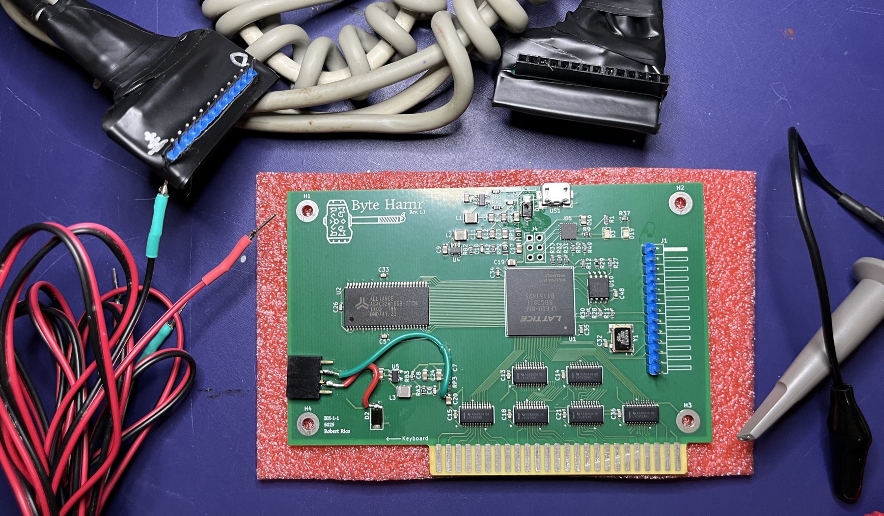
Then the data bus. Both sides of the data level shifter were driving at once. The transceiver DIR pin needed the inverse of R/W and was getting R/W straight. Field surgery: one 74F04 dead-bugged onto the board, several questionable solder joints, and enough bodge wire to show this is my second PCB. She ain’t pretty, but she works.
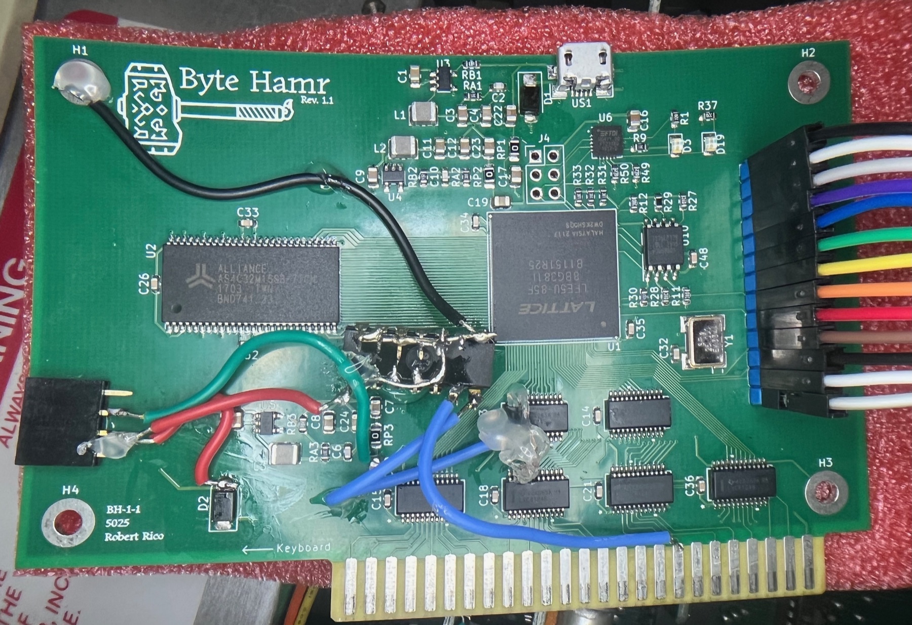
What I measured
- Read and write cycles work between the IIe and the FPGA.
- The IIe can read and write the onboard SDRAM through the card.
What broke or surprised me
Three weeks of 6502 code had been debugged against a data bus that was fighting itself. Some of that debugging was chasing the hardware.
Next
Rev 2 header layout. The suggestion from the thread was a two-row header with one row all ground, placed at the keyboard end so a perfboard daughtercard can hang off it. I want probe access to the outside world for the analyzer, which pushes toward the back edge like the Disk II controller. Current thinking is one 34 or 40-pin IDC header at the back edge with signals, 3.3 V, 5 V and 12 V, maybe the negatives, and interleaved grounds. I would rather expose a bare minimum and let people extend it than put an SD slot and an ESP32 on the board.